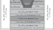
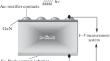
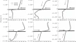
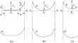
Investigation of DC and RF Performance of Novel MOSHEMT on Silicon Substrate for Future Submillimetre Wave Applications J. AjayanT. RavichandranD. Nirmal PHYSICS OF SEMICONDUCTOR DEVICES 26 February 2019 Pages: 1991 - 1997
Simulation and Experimental Studies of Illumination Effects on the Current Transport of Nitridated GaAs Schottky Diode A. RabehiM. AmraniC. Robert-Goumet PHYSICS OF SEMICONDUCTOR DEVICES 26 February 2019 Pages: 1998 - 2006
Diode Polarization and Resistive Switching in Metal/TlGaSe2 Semiconductor/Metal Devices MirHasan Yu. SeyidovR. A. SuleymanovBuket Bilgen Kandemir PHYSICS OF SEMICONDUCTOR DEVICES 26 February 2019 Pages: 2007 - 2016
Investigation of InGaAs/GaAs Quantum Well Lasers with Slightly Doped Tunnel Junction Yajie LiPengfei WangJiaoqing Pan SEMICONDUCTOR STRUCTURES, LOW-DIMENSIONAL SYSTEMS, AND QUANTUM PHENOMENA 26 February 2019 Pages: 2017 - 2021
Critical Radius of Full Depletion in Semiconductor Nanowires Caused by Surface Charge Trapping S. G. PetrosyanA. E. YesayanV. A. Khachatryan SEMICONDUCTOR STRUCTURES, LOW-DIMENSIONAL SYSTEMS, AND QUANTUM PHENOMENA 26 February 2019 Pages: 2022 - 2025
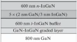
Near-Infrared InGaN Alloys Grown on High-In-Composition InGaN Buffer Layer Lianhong YangFuqiang GuoDunjun Chen SURFACES, INTERFACES, AND THIN FILMS 26 February 2019 Pages: 2026 - 2029
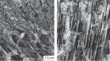
Microstructural Evolution of MOVPE Grown GaN by the Carrier Gas I. DemirI. AltuntasS. Elagoz SURFACES, INTERFACES, AND THIN FILMS 26 February 2019 Pages: 2030 - 2038
Structural, Thermal and Luminescence Properties of AlN:Tm Thin Films Deposited on Silicon Substrate and Optical Fiber Muhammad MaqboolAmani AlruwailiIftikhar Ahmad SURFACES, INTERFACES, AND THIN FILMS 26 February 2019 Pages: 2039 - 2045
Stable and Unstable Spatial Modes in a Resonator with a Half-Disk Shape M. S. DunaevskiyP. A. AlekseevR. Teissier 26th INTERNATIONAL SYMPOSIUM “NANOSTRUCTURES: PHYSICS AND TECHNOLOGY”. NANOSTRUCTURE CHARACTERIZATION 26 February 2019 Pages: 2046 - 2048
Reflectometry of X-ray Whispering Gallery Waves Propagating along Liquid Meniscuses L. I. GorayV. E. AsadchikovA. M. Tikhonov 26th INTERNATIONAL SYMPOSIUM “NANOSTRUCTURES: PHYSICS AND TECHNOLOGY”. NANOSTRUCTURE CHARACTERIZATION 26 February 2019 Pages: 2049 - 2053
Polarization Properties of Photoluminescence of Anisotropic Polymer Films Containing Aligned Au Nanorods and Semiconductor Nanoparticles of Various Shape L. I. GurinovichL. L. TrotsiukS. V. Gaponenko 26th INTERNATIONAL SYMPOSIUM “NANOSTRUCTURES: PHYSICS AND TECHNOLOGY”. NANOSTRUCTURE CHARACTERIZATION 26 February 2019 Pages: 2054 - 2056
Сomposition Depth Profiling of the GaAs Native Oxide Irradiated by an Ar+ Ion Beam V. M. MikoushkinV. V. BryzgalovD.E. Marchenko 26th INTERNATIONAL SYMPOSIUM “NANOSTRUCTURES: PHYSICS AND TECHNOLOGY”. NANOSTRUCTURE CHARACTERIZATION 26 February 2019 Pages: 2057 - 2060
In situ Bandgap Determination of the GaAsN Nanolayer Prepared by Low-Energy \({\text{N}}_{2}^{ + }\) Ion Implantation V. M. Mikoushkin 26th INTERNATIONAL SYMPOSIUM “NANOSTRUCTURES: PHYSICS AND TECHNOLOGY”. NANOSTRUCTURE CHARACTERIZATION 26 February 2019 Pages: 2061 - 2064
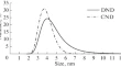
Atomic Force Microscopy Study of Monodisperse Carbon Nanoparticles D. V. MuravijovaI. A. ErmakovM. V. Baidakova 26th INTERNATIONAL SYMPOSIUM “NANOSTRUCTURES: PHYSICS AND TECHNOLOGY”. NANOSTRUCTURE CHARACTERIZATION 26 February 2019 Pages: 2065 - 2067
Polarized Retroreflection from Nanoporous III–V Semiconductors S. Ya. PrislopskiS. V. GaponenkoI. M. Tiginyanu 26th INTERNATIONAL SYMPOSIUM “NANOSTRUCTURES: PHYSICS AND TECHNOLOGY”. NANOSTRUCTURE CHARACTERIZATION 26 February 2019 Pages: 2068 - 2069
XAFS Investigation of Nanoparticle Formation in 64Zn+ Ion Implanted and Thermo Oxidized Si E. V. KhramovV. V. Privezentsev 26th INTERNATIONAL SYMPOSIUM “NANOSTRUCTURES: PHYSICS AND TECHNOLOGY”. NANOSTRUCTURE CHARACTERIZATION 26 February 2019 Pages: 2070 - 2072
Growth of Textured Au–Fe/Fe Hybrid Nanocrystals on Oxidized Silicon Surface I. A. TarasovT. E. SmolyarovaS. G. Ovchinnikov 26th INTERNATIONAL SYMPOSIUM “NANOSTRUCTURES: PHYSICS AND TECHNOLOGY”. NANOSTRUCTURE CHARACTERIZATION 26 February 2019 Pages: 2073 - 2077
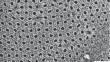
Influence of the Pore Structure on the Electron Barrier Height of Metal-Ceramic Nanomaterials Based on Gold-Anodic Aluminum Oxide N. M. UshakovM. Yu. Vasil’kovV. R. Shaturnuy 26th INTERNATIONAL SYMPOSIUM “NANOSTRUCTURES: PHYSICS AND TECHNOLOGY”. NANOSTRUCTURE CHARACTERIZATION 26 February 2019 Pages: 2078 - 2080
Atomic Force Microscopy Local Oxidation of GeO Thin Films K. N. AstankovaA. S. KozhukhovA. V. Latyshev 26th INTERNATIONAL SYMPOSIUM “NANOSTRUCTURES: PHYSICS AND TECHNOLOGY”. NANOSTRUCTURE TECHNOLOGY 26 February 2019 Pages: 2081 - 2084
Growth Modes of GaN Plasma-Assisted MBE Nanowires Yu. S. BerdnikovN. V. Sibirev 26th INTERNATIONAL SYMPOSIUM “NANOSTRUCTURES: PHYSICS AND TECHNOLOGY”. NANOSTRUCTURE TECHNOLOGY 26 February 2019 Pages: 2085 - 2087
Microlens-Enhanced Substrate Patterning and MBE Growth of GaP Nanowires A. D. BolshakovL. N. DvoretckaiaI. S. Mukhin 26th INTERNATIONAL SYMPOSIUM “NANOSTRUCTURES: PHYSICS AND TECHNOLOGY”. NANOSTRUCTURE TECHNOLOGY 26 February 2019 Pages: 2088 - 2091
Self-Catalyzed MBE-Grown GaP Nanowires on Si(111): V/III Ratio Effects on the Morphology and Crystal Phase Switching V. V. FedorovA. D. BolshakovI. S. Mukhin 26th INTERNATIONAL SYMPOSIUM “NANOSTRUCTURES: PHYSICS AND TECHNOLOGY”. NANOSTRUCTURE TECHNOLOGY 26 February 2019 Pages: 2092 - 2095
InGaN/GaN QDs Nanorods: Processing and Properties K. P. KotlyarI. P. SoshnikovV. V. Lysak 26th INTERNATIONAL SYMPOSIUM “NANOSTRUCTURES: PHYSICS AND TECHNOLOGY”. NANOSTRUCTURE TECHNOLOGY 26 February 2019 Pages: 2096 - 2098
Formation and Properties of New Types of Metal–Dielectric Nanostructures for Creating Optical Metamaterials N. S. KazakV. E. AgabekovV. N. Belyi 26th INTERNATIONAL SYMPOSIUM “NANOSTRUCTURES: PHYSICS AND TECHNOLOGY”. NANOSTRUCTURE TECHNOLOGY 26 February 2019 Pages: 2099 - 2102
New Advanced Hybrid Organic–Inorganic Complex V. A. LapinaT. A. PavichP. P. Pershukevich 26th INTERNATIONAL SYMPOSIUM “NANOSTRUCTURES: PHYSICS AND TECHNOLOGY”. NANOSTRUCTURE TECHNOLOGY 26 February 2019 Pages: 2103 - 2106
MBE AlGaN/GaN HEMT Heterostructures with Optimized AlN Buffer on Al2O3 E. V. LutsenkoM. V. RzheutskiG. P. Yablonskii 26th INTERNATIONAL SYMPOSIUM “NANOSTRUCTURES: PHYSICS AND TECHNOLOGY”. NANOSTRUCTURE TECHNOLOGY 26 February 2019 Pages: 2107 - 2110
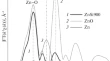
Structural Transformation of “Silica+Zn” Nanocomposite after Annealing in Oxidizing Atmosphere F. F. KomarovM. A. MakhavikouJ. Żuk 26th INTERNATIONAL SYMPOSIUM “NANOSTRUCTURES: PHYSICS AND TECHNOLOGY”. NANOSTRUCTURE TECHNOLOGY 26 February 2019 Pages: 2111 - 2113
FIB Lithography Challenges of Si3N4/GaN Mask Preparation for Selective Epitaxy M. I. MitrofanovI. V. LevitskiiM.N. Mizerov 26th INTERNATIONAL SYMPOSIUM “NANOSTRUCTURES: PHYSICS AND TECHNOLOGY”. NANOSTRUCTURE TECHNOLOGY 26 February 2019 Pages: 2114 - 2116
Processing of GaN/Si(111) Epitaxial Structures for MEMS Applications K. Yu. ShubinaT. N. BerezovskayaA. D. Bouravleuv 26th INTERNATIONAL SYMPOSIUM “NANOSTRUCTURES: PHYSICS AND TECHNOLOGY”. NANOSTRUCTURE TECHNOLOGY 26 February 2019 Pages: 2117 - 2119
Estimation of Evaporation Rate from Gold-Silicon Alloy Based on the Nucleation Time and Nanowire Length Distributions N. V. SibirevV. V. BelyaevY. S. Berdnikov 26th INTERNATIONAL SYMPOSIUM “NANOSTRUCTURES: PHYSICS AND TECHNOLOGY”. NANOSTRUCTURE TECHNOLOGY 26 February 2019 Pages: 2120 - 2123
Two Methods of Calculation Ternary Nanowire Composition N. V. SibirevA. A. KoryakinY. S. Berdnikov 26th INTERNATIONAL SYMPOSIUM “NANOSTRUCTURES: PHYSICS AND TECHNOLOGY”. NANOSTRUCTURE TECHNOLOGY 26 February 2019 Pages: 2124 - 2127
Heteroepitaxy of GaP Nucleation Layers on Si by Molecular Beam Epitaxy M. S. SobolevA. A. LazarenkoA. D. Bouravleuv 26th INTERNATIONAL SYMPOSIUM “NANOSTRUCTURES: PHYSICS AND TECHNOLOGY”. NANOSTRUCTURE TECHNOLOGY 26 February 2019 Pages: 2128 - 2131
Nucleation and Growth Modeling of Protein Crystals in Capillaries A. S. SokolovskiiN. A. BesedinaV. G. Dubrovskii 26th INTERNATIONAL SYMPOSIUM “NANOSTRUCTURES: PHYSICS AND TECHNOLOGY”. NANOSTRUCTURE TECHNOLOGY 26 February 2019 Pages: 2132 - 2134
Monte Carlo Simulation of Ga Droplet Movement during the GaAs Langmuir Evaporation A. A. SpirinaA. G. NastovjakN. L. Shwartz 26th INTERNATIONAL SYMPOSIUM “NANOSTRUCTURES: PHYSICS AND TECHNOLOGY”. NANOSTRUCTURE TECHNOLOGY 26 February 2019 Pages: 2135 - 2139
Luminescent Silicon Nanocrystals Prepared by Laser-Assisted Synthesis in Liquid for Imaging and Photovoltaic Applications N. V. TarasenkoA. V. ButsenG. Račiukaitis 26th INTERNATIONAL SYMPOSIUM “NANOSTRUCTURES: PHYSICS AND TECHNOLOGY”. NANOSTRUCTURE TECHNOLOGY 26 February 2019 Pages: 2140 - 2142
Manganese Doped Zinc Sulfide Quantum Dots as Efficient Photocatalyst for Dye Decolorization K. A. SergeevaA. A. SergeevS. S. Voznesenskiy 26th INTERNATIONAL SYMPOSIUM “NANOSTRUCTURES: PHYSICS AND TECHNOLOGY”. QUANTUM WELLS AND QUANTUM DOTS 26 February 2019 Pages: 2143 - 2145
Structural and Optical Properties of Wurtzite AlGaAs Nanowires Grown by MBE on Si(111) Substrate I. V. ShtromK. P. KotlyarG. E. Cirlin 26th INTERNATIONAL SYMPOSIUM “NANOSTRUCTURES: PHYSICS AND TECHNOLOGY”. QUANTUM WELLS AND QUANTUM DOTS 26 February 2019 Pages: 2146 - 2148
Plasmonic Enhancement of the Photoluminescence in Hybrid Structures with SiGe Quantum Dots and Ag Nanoislands V. A. ZinovyevA. F. ZinovievaA. V. Mudryi 26th INTERNATIONAL SYMPOSIUM “NANOSTRUCTURES: PHYSICS AND TECHNOLOGY”. QUANTUM WELLS AND QUANTUM DOTS 26 February 2019 Pages: 2149 - 2152