Effect of Nickel and Copper Introduced at Room Temperature on the Recombination Properties of Extended Defects in Silicon V. I. OrlovN. A. YarykinE. B. Yakimov NONELECTRONIC PROPERTIES OF SEMICONDUCTORS (ATOMIC STRUCTURE, DIFFUSION) 06 May 2019 Pages: 411 - 414
Defect Formation under Nitrogen-Ion Implantation and Subsequent Annealing in GaAs Structures with an Uncovered Surface and a Surface Covered with an AlN Film N. A. SobolevV. I. SakharovE. V. Sherstnev NONELECTRONIC PROPERTIES OF SEMICONDUCTORS (ATOMIC STRUCTURE, DIFFUSION) 06 May 2019 Pages: 415 - 418
Thermoelectric Characteristics of Heavily Doped p-Type Lead Telluride at Different Heavy-Hole Band Depths A. V. Dmitriev ELECTRONIC PROPERTIES OF SEMICONDUCTORS 06 May 2019 Pages: 419 - 427
Carrier Lifetime in Semiconductors with Band-Gap Widths Close to the Spin-Orbit Splitting Energies N. L. BazhenovK. D. MynbaevG. G. Zegrya SPECTROSCOPY, INTERACTION WITH RADIATION 06 May 2019 Pages: 428 - 433
Evolution of Micropits on Large Terraces of the Si(111) Surface during High-Temperature Annealing A. S. PetrovS. V. SitnikovA. V. Latyshev SURFACES, INTERFACES, AND THIN FILMS 06 May 2019 Pages: 434 - 438
Effect of a Second-Order Phase Transition on the Electrical Conductivity of Metal/Semiconductor Structures I. R. NabiullinR. M. GadievA. N. Lachinov SURFACES, INTERFACES, AND THIN FILMS 06 May 2019 Pages: 439 - 441
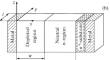
Simulated Contrast of Two Dislocations M. LedraA. El Hdiy SURFACES, INTERFACES, AND THIN FILMS 06 May 2019 Pages: 442 - 446
Preparation and Characterization of Sol–Gel Dip Coated Al: ZnO (AZO) Thin Film for Opto-Electronic Application K. Deva Arun KumarS. ValanarasuS. Rex Rosario SURFACES, INTERFACES, AND THIN FILMS 06 May 2019 Pages: 447 - 451
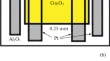
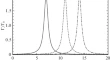
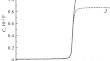
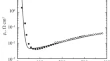
Influence of the Substrate Material on the Properties of Gallium-Oxide Films and Gallium-Oxide-Based Structures V. M. KalyginaT. Z. LygdenovaE. V. Chernikov SEMICONDUCTOR STRUCTURES, LOW-DIMENSIONAL SYSTEMS, AND QUANTUM PHENOMENA 06 May 2019 Pages: 452 - 457
Resonance Absorption of Electromagnetic Radiation in a Phosphorene Single Layer V. V. KarpuninV. A. Margulis SEMICONDUCTOR STRUCTURES, LOW-DIMENSIONAL SYSTEMS, AND QUANTUM PHENOMENA 06 May 2019 Pages: 458 - 464
Features of the Characteristics of Field-Resistant Silicon–Ultrathin Oxide–Polysilicon Structures E. I. GoldmanS. A. LevashovG. V. Chucheva SEMICONDUCTOR STRUCTURES, LOW-DIMENSIONAL SYSTEMS, AND QUANTUM PHENOMENA 06 May 2019 Pages: 465 - 468
Features of the Temperature Dependence of the Specific Contact Resistance of Au–Ti–Pd–n+–n-Si Diffusion Silicon Structures A. E. BelyaevN. S. BoltovetsA. V. Sachenko SEMICONDUCTOR STRUCTURES, LOW-DIMENSIONAL SYSTEMS, AND QUANTUM PHENOMENA 06 May 2019 Pages: 469 - 476
Investigation into the Distribution of Built-in Electric Fields in LED Heterostructures with Multiple GaN/InGaN Quantum Wells by Electroreflectance Spectroscopy A. E. AslanyanL. P. AvakyantsA. V. Chervyakov SEMICONDUCTOR STRUCTURES, LOW-DIMENSIONAL SYSTEMS, AND QUANTUM PHENOMENA 06 May 2019 Pages: 477 - 483
Quantum Confined Stark Effect and Temperature Dependencies of Photoluminescence of InAs Quantum Dots Coupled with AlGaAs/GaAs Two Dimensional Electron Gas H. KhmissiA. M. El Sayed SEMICONDUCTOR STRUCTURES, LOW-DIMENSIONAL SYSTEMS, AND QUANTUM PHENOMENA 06 May 2019 Pages: 484 - 488
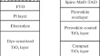
Electrical Characterization of Hybrid Halide Perovskites Based Heterojunction Device Jyoti ChaudharyShaily ChoudharyAjay Singh Verma SEMICONDUCTOR STRUCTURES, LOW-DIMENSIONAL SYSTEMS, AND QUANTUM PHENOMENA 06 May 2019 Pages: 489 - 492
Raman Scattering in InSb Spherical Nanocrystals Ion-Synthesized in Silicon-Oxide Films I. E. TyschenkoV. A. VolodinV. P. Popov MICROCRYSTALLINE, NANOCRYSTALLINE, POROUS, AND COMPOSITE SEMICONDUCTORS 06 May 2019 Pages: 493 - 498
Optical Properties of CdSe/ZnS Nanoparticles in Heat-Treated Polyvinylchloride Films S. I. RasmaginI. K. Novikov MICROCRYSTALLINE, NANOCRYSTALLINE, POROUS, AND COMPOSITE SEMICONDUCTORS 06 May 2019 Pages: 499 - 502
The Growth of InAsxSb1 –x Solid Solutions on Misoriented GaAs(001) Substrates by Molecular-Beam Epitaxy E. A. EmelyanovA. V. VasevV. V. Preobrazhenskii MICROCRYSTALLINE, NANOCRYSTALLINE, POROUS, AND COMPOSITE SEMICONDUCTORS 06 May 2019 Pages: 503 - 510
Large-Amplitude Shock Electromagnetic Wave in a Nonlinear Transmission Line Based on a Distributed Semiconductor Diode A. S. Kyuregyan PHYSICS OF SEMICONDUCTOR DEVICES 06 May 2019 Pages: 511 - 518
High-Power Nano- and Picosecond Optoelectronic Switches Based on High-Voltage Silicon Structures with p–n Junctions. III. Self-Heating Effects A. S. Kyuregyan PHYSICS OF SEMICONDUCTOR DEVICES 06 May 2019 Pages: 519 - 523
Inhomogeneous Injection and Heat-Transfer Processes in Reversely Switched Dynistors Operating in the Pulse-Frequency Repetition Modes with a Limited Heat Sink A. V. GorbatyukB. V. Ivanov PHYSICS OF SEMICONDUCTOR DEVICES 06 May 2019 Pages: 524 - 529
Formation of Porous Silicon by Nanopowder Sintering E. V. AstrovaV. B. VoronkovYu. A. Kukushkina PHYSICS OF SEMICONDUCTOR DEVICES 06 May 2019 Pages: 530 - 539
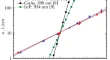
Power Conversion Efficiencies of Perovskite and Dye-Sensitized Solar Cells under Various Solar Radiation Intensities A. B. NikolskaiaS. S. KozlovO. I. Shevaleevskiy PHYSICS OF SEMICONDUCTOR DEVICES 06 May 2019 Pages: 540 - 544
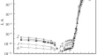
Effect of Electron Irradiation with an Energy of 0.9 MeV on the I–V Characteristics and Low-Frequency Noise in 4H–SiC pin Diodes V. A. DobrovV. V. KozlovskiN. M. Shmidt PHYSICS OF SEMICONDUCTOR DEVICES 06 May 2019 Pages: 545 - 551
Electrical and Optical Characteristics of Si-Nanoparticle Films Deposited onto Substrates by High-Voltage Electrospraying from Ethanol Sols N. N. KononovD. V. DavydovaS. G. Dorofeev FABRICATION, TREATMENT, AND TESTING OF MATERIALS AND STRUCTURES 06 May 2019 Pages: 552 - 565
Optical and Structural Properties of Ag and c-Si Nanostructures Formed During the Metal-Assisted Chemical Etching of Silicon Yu. A. ZharovaV. A. TolmachevS. I. Pavlov FABRICATION, TREATMENT, AND TESTING OF MATERIALS AND STRUCTURES 06 May 2019 Pages: 566 - 572
Effect of Oxygen Flow Rate on Structural, Electrical and Optical Properties of Zinc Aluminum Oxide Thin Films Deposited by DC Magnetron Sputtering B. Rajesh KumarB. Hymavathi FABRICATION, TREATMENT, AND TESTING OF MATERIALS AND STRUCTURES 06 May 2019 Pages: 573 - 581