
Abstract
Safety-critical systems have to follow extremely high dependability requirements as specified in the standards for automotive, air, and space applications. The required high fault coverage at runtime is usually obtained by a combination of concurrent error detection or correction and periodic tests within rather short time intervals. The concurrent scheme ensures the integrity of computed results while the periodic test has to identify potential aging problems and to prevent any fault accumulation which may invalidate the concurrent error detection mechanism. Such periodic built-in self-test (BIST) schemes are already commercialized for memories and for random logic. The paper at hand extends this approach to interconnect structures. A BIST scheme is presented which targets interconnect defects before they will actually affect the system functionality at nominal speed. A BIST schedule is developed which significantly reduces aging caused by electromigration during the lifetime application of the periodic test.
1 Introduction
Functional safety is a key concern in autonomous systems. In the automotive domain, for example, the ISO 26262 standard defines clear targets for test and reliability that drive research and development in the industry [16, 35, 38]. First of all, the manufacturing test must ensure a high product quality by reducing test escapes to a minimum (“zero defect strategy”). During operation, safety critical systems are typically protected by error correcting codes and other techniques for concurrent testing. However, safety-critical systems, such as anti-blocking brakes, may also have longer idle time, where faults cannot be detected by concurrent testing. Similarly, stand-by spare parts are not used during normal operation, but their health status must be maintained. To avoid fault accumulation during idle times, built-in tests are needed which can be triggered periodically. For logic circuits, quite a few approaches are already available addressing these specific requirements. They range from dedicated BIST and observation schemes [28, 33] to applications of software-based self-test [5, 42]. Similarly, schemes for embedded memories rely on scrubbing [30] and periodic consistency checking [19] in addition to the protection by the error detecting and correcting codes.
However, in today’s complex systems, the reliability of the long interconnects between the components has also become a major concern. The severe impact of technology scaling on the signal integrity in bus structures or network on chip (NoC) links [9] has triggered research on advanced interconnect testing. Here specific defect and aging mechanisms such as crosstalk or electromigration (EM) must be addressed, which can manifest themselves for example as delay faults or glitches at the gate level. In this context, the BIST and monitoring schemes proposed in [4, 11, 17, 32, 34, 36, 37, 41, 47, 49, 55, 56], focus on manufacturing test, but they do not address the requirements and challenges of health monitoring during the lifetime. Nevertheless, because of the complex interplay between EM and crosstalk, periodic testing of interconnects is mandatory and at the same time extremely challenging. On the one hand, EM may change the interconnect geometry and lead to increased crosstalk effects. On the other hand, the crosstalk-induced currents can in turn aggravate EM [29], and even small crosstalk effects can constitute reliability risks that must be considered [45].
The available interconnect BIST schemes for manufacturing testing cannot be directly applied, because they mainly target “large” crosstalk effects which change the system data. Furthermore, each test execution itself adds stress to the interconnects. In periodic testing, this stress can accumulate and lead to accelerated aging. Consequently, in a safety critical system, where a reliability above a given threshold has to be guaranteed, the test must be carefully designed to minimize its negative impact on the mission time. In particular, in the case of stand-by spare parts, a sufficient mission time after a reconfiguration must be ensured.
Degradation caused by EM has been studied extensively in the context of chip design [7, 8, 14, 15, 31], and EM-aware design techniques exploit self-healing mechanisms triggered by reversed current [24]. In particular, work on EM-aware routing in NoCs addresses the problem of stress accumulation by packet transmission over the network links [20]. To exploit self-healing by a reversed current, a dynamic routing strategy balances the number of packets that are sent and received over a link. Such an EM-aware routing scheme can easily be combined with test and diagnosis schemes for NoCs reusing the NoC infrastructure [17, 50].
In this paper, a new approach for periodic EM-aware test will be presented, which is applicable to general bi-directional interconnect structures at the system level. It can identify and classify reliability risks before they actually cause a failure. At the same time, the proposed EM-aware strategy maximizes the mission time of the system. Similar to the dynamic routing strategy in [20], it tries to properly balance senders and receivers during test. The scheme is based on a multi-frequency test, which not only detects failures, but also provides a reliability profile of the interconnect structures. The periodic update of this reliability profiles supports a dynamic test scheduling, where the direction of the test is changed whenever the accumulated stress gets too high.
Before the proposed strategy is explained in more detail, the necessary background is provided in Sect. 2. Subsequently, Sect. 3 analyzes the impact of the periodic test on electromigration. Section 4 introduces the basic BIST architecture. Finally, Sect. 5 deals with the proper tuning of this architecture and explains the developed concepts for test scheduling. The experimental results in Sect. 6 will show that the developed stress-aware test improves the mission times by orders of magnitude compared to a straightforward approach.
2 Background
This section briefly summarizes the necessary background on interconnect modeling and test, the relation between coupling and electromigration, as well as the multi-frequency test scheme introduced in [45].
-
A.
Interconnect and Fault Modeling
Interconnect lines will be modeled as a sequence of RLC circuits [10, 13, 43]. As an example, Fig. 1 shows one segment of a three-lines interconnect. Each wire i is characterized by its capacitance to other layers Ci, inductance Li, and resistance Ri. Between every two wires i and j, there are also coupling capacitances Cij, inductances Lij, and resistances Rij depending on the space between the wires.
Fig. 1 
Model for on-chip communication [13]
Coupling between lines leads to crosstalk effects such as glitches, delay and speedy faults, and also overshoots and undershoots. The amplitudes of glitch distortions and of the overshoots and undershoots as well as the delay sizes depend on the strength of the coupling elements.
Crosstalk effects are usually described as a signal distortion on a victim line caused by a transition on one or more aggressor lines. Several fault models have been proposed to support crosstalk analysis and test at higher levels of abstraction. The maximum aggressor (MA) model assumes that the worst-case effect on a single victim line is provoked when all other lines act as aggressors in the same way [13]. However, this model does not consider the impact of inductances and does not always correctly reflect the worst case. To overcome the disadvantages of the MA model, some authors suggest to use pseudo-random patterns for signal integrity test [36]. Nevertheless, shorter test times can be ensured with advanced deterministic approaches. The maximum transition (MT) fault model combines a transition or a stable signal on a victim line with multiple transitions on a limited number of aggressor lines [55]. Based on the analysis of the combined effect of capacitances and inductances, the maximal dominant signal integrity (MDSI) fault model also works with a limited number of aggressors but derives conditions for the remaining lines in addition to that [12].
The MDSI model allows for a very simple deterministic test with only a few pattern pairs. Table 1 summarizes the necessary pattern pairs for a complete crosstalk test of one victim line. To test the victim for delays, glitches, and speedy faults, 6 pattern pairs are sufficient. As the MDSI fault model assumes that only one victim at a time is addressed, in total 6·N (possibly overlapping) pattern pairs are needed for an N-bit interconnect.
Table 1 Complete MDSI test of one victim line A more efficient test scheme based on multiple victim testing (MVT) is proposed in [37] and used in this paper. The conditions for the signals on the victim and aggressor lines are the same as in the MDSI model, and working with several victim lines has a similar effect as the conditions for the remaining lines in the MDSI model. An example is shown in Fig. 2, where the two victim lines v1 and v2 (blue lines) are tested in parallel for crosstalk delays by activating the inverse transitions on the neighboring aggressor lines (red lines).
Fig. 2 
Test for crosstalk delays
-
B.
Interconnect BIST
While many existing schemes for interconnect BIST rely on a serial transmission of test data within a boundary scan environment, the presented work deals with the parallel test application in SoCs. The short overview in this section therefore focuses on the main ideas and skips details on boundary-scan integration.
Early approaches on interconnect BIST mainly address manufacturing defects modeled as shorts, stuck-opens, and stuck-at faults [18]. Counter sequences, walking ones, or LFSR-based pseudo-random sequences are generated serially by respective test pattern generators.
With the increasing progress in technology, interconnect performance and signal integrity have become predominant. Bai et al. describe an approach for generating deterministic patterns based on the MA model [4]. A small finite state machine produces the proper transitions for the victim line and the aggressor lines, which are then distributed to the interconnect via multiplexers. Sekar and Dey also base their analysis on the MA model but suggest to re-use the LFSR typically available for logic BIST [49]. To guarantee a high fault coverage with an acceptable number of patterns the LFSR-outputs are modified by some extra logic. In [11] a software-based self-test relying on MA patterns is proposed.
To avoid the problems related to the MA model, an LFSR is used as a pseudo-random pattern generator in [36]. Furthermore, special receiver cells for interconnect BIST based on sense amplifiers are presented. Similarly, Pendurkar et al. build on small pre-characterized LFSRs which are combined to mimic the switching activity of the interconnect in system mode [41]. Other authors promote a pseudo-exhaustive test, where all possible combinations of transitions are applied to groups of lines, or even an exhaustive test, in case the interconnect topology is unknown [27, 44]. Both approaches use LFSRs for pattern generation. Deterministic approaches for advanced fault models integrate tests based on the MT and the MDSI model [32, 56].
A parallel BIST scheme for testing manufacturing defects is presented in [23]. It uses a simple circular shift register as the core of a parallel BIST scheme. In section IV a parallel generator for the periodic crosstalk test will be introduced for multiple victim test.
-
C.
Reliability Measures
In this work the specification and evaluation of reliability properties rely on common fault tolerance concepts and terminology. As a more in-depth introduction is beyond the scope of this paper, the reader is referred to respective textbooks, e.g. [22].
The reliability R(t) is formally defined as the probability that a system survives from time 0 to t. For safety critical systems, it is typically required that R(t) is above a given threshold Rth, and the mission time TM(Rth) is defined as time span where R(t) ≥ Rth holds. Changes in the design or test strategy are then evaluated by the mission time improvement factor
$$MTIF ={T}_{M}^{new}({R}_{th})/{T}_{M}^{old}\left({R}_{th}\right).$$(1)If the mission times cannot be determined directly, they can be computed with the help of the median time to failure t50 or the more common mean time to failure MTTF as shown in the following.
If a constant failure rate λ is assumed, then
$$R\left(t\right)={e}^{-\lambda t}, {\text {and}}\; MTTF=\frac{1}{\lambda }$$(2)hold [22]. The median time to failure is the time when 50% of the interconnects fail, i.e. the reliability is R(t50) = 1/2. Using Eq. (2), it can be shown that
$${t}_{50}=MTTF\cdot ln\left(2\right),$$(3)and similarly
$${T}_{M}=-MTTF\cdot ln\left({R}_{th}\right)=-\frac{{t}_{50}}{\mathit{ln}\left(2\right)}\cdot ln\left({R}_{th}\right).$$(4)Therefore, the mission time improvement can also be estimated as
$$MTIF= \frac{{MTTF}^{new}}{{MTTF}^{old}}= \frac{{t}_{50}^{new}}{{t}_{50}^{old}}.$$(5) -
D.
Coupling and Electromigration
As shown in [29], crosstalk can aggravate EM and thus reduce the reliability of the system. This is not only true for crosstalk effects actually changing the functionality of the system [45]. Even if the crosstalk noise only leads to small delays within the design margin, it can trigger EM. Such small crosstalk faults remain undetected by tests at the nominal frequency and are therefore called hidden interconnect defects.
The relation between coupling and EM, in particular in the presence of variations in the line spacing, will be summarized in the following. EM refers to the transportation of metal ions caused by an electrical field. For a detailed introduction into various aspects of EM in integrated circuit design, the reader is referred to the textbook of Lienig and Thiele [24]. The metal ion transport is reshaping interconnect lines over time. This, in turn, changes the resistance of interconnects and can lead to increased interconnect delays [31]. Furthermore, several studies have shown that EM can cause serious failures by creating hillocks and voids in the interconnect lines [15]. In the worst case, a hillock can become a bridging fault between adjacent wires, and a void can result in a broken line.
The impact of EM on the system is typically characterized by the median time to failure t50. According to Black’s Formula, t50 measured in hours can be estimated based on the physical parameters of the system as
$${t}_{50}=\frac{A}{{j}^{n }}{e}^{{E}_{a}/{k}_{B}\cdot T},$$(6)where A is a constant depending on the cross-section of the wire, j is the current density in amperes per square centimeter, n is a constant related to the material, Ea is the activation energy in electron volts, kB is the Boltzmann constant and T is the temperature in degrees Kelvin [7, 8, 48, 57]. The material constant n is typically between 1 and 2, e.g. 1.1–1.3 for copper and 2 for aluminum [24].
When the parameters j and T change, the mission time improvement is obtained as
$$MTIF={\left(\frac{{j}^{old}}{{j}^{new}}\right)}^{n}exp(\frac{{E}_{a}}{{k}_{B}}\left(\frac{1}{{T}^{new}}-\frac{1}{{T}^{old}}\right))$$(7)by inserting Formula (6) into Eq. (5).
As Eqs. (6) and (7) show, in addition to the temperature, the current density j has a major impact on EM effects and on the resulting changes in mission time.
For a given cross-section, the current density is defined as the amount of charge per unit time that flows through a unit area. It can be estimated by
$$j=\frac{{I}_{avg}}{W\cdot H}.$$(8)The parameters W and H denote the width and the height of the wire, and Iavg is the average current. The average current Iavg can be determined by simulations or analytically, e.g. using the techniques in [3, 6]. In CMOS technology, the dynamic power is dominant, therefore the average current can be estimated as Iavg = C·Vdd·f·p, where C is the capacitance of the wire, Vdd is the supply voltage, f is the clock frequency, and p is the switching probability [2]. The current density is then obtained as
$$j=\frac{C\cdot {V}_{dd}\cdot f\cdot p}{W\cdot H}.$$(9)As coupling effects strongly depend on the line spacing, a realistic analysis of the induced average current must take into account variations of the interconnect layout. For this, in [45] variations in the line spacing have been analyzed ranging from 100% down to 80% of the nominal value. Simulation results for 80% of the nominal line spacing in 32 nm technology have shown more than a 20% increase of the coupling capacitance and more than a 7% increase of the coupling inductance for typical crosstalk patterns. A line spacing below 80% of the nominal value has not been considered, because this would result in large crosstalk faults which change the functionality of the system and could be easily detected.
Figure 3 summarizes the impact of variations in the wire spacing on the average current for the 32 and 45 nm technologies and a glitch pattern 000 → 101 applied to a 3-line interconnect (source voltage is 0.9 V). The horizontal axis shows variations in the line spacing ranging from 100% down to 80% of the nominal value, and the vertical axis shows the increase in current for the glitch pattern relative to the situation with nominal line spacing.
Fig. 3 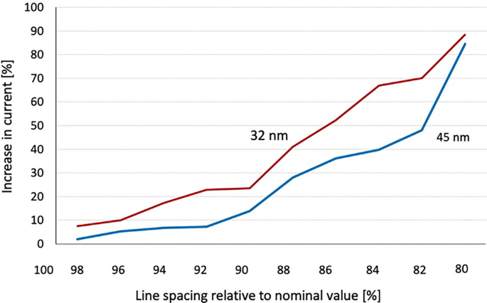
The average current increment for varying line spacing
It can be observed that the changes in current evolve almost linearly with the increasing coupling capacitances and inductances caused by a reduced line spacing. In particular, the curve for the 32 nm technology shows that already small variations in the line spacing can increase the current by almost 10%, and their contribution to EM cannot be neglected. Therefore, both manufacturing and periodic in-system test must also address hidden interconnect defects to identify possible reliability threats, before they actually cause a failure.
-
E.
Dynamic Multi-frequency Test
As shown in Sect. 2C, already small variations in the line spacing have a non-negligible impact on EM. As the resulting crosstalk faults may be hidden at the nominal frequency, they must be tested at higher frequencies. The approach in [45] uses several frequencies to characterize the risk of EM-degradation by crosstalk-induced delays. The main ideas are briefly summarized with the help of the pseudo-code in Fig. 4.
Fig. 4 
Multi-frequency test
The multi-frequency test starts with a delay test for all lines L at the nominal frequency f0 = fnom. In each iteration i, the frequency is increased to the next frequency fi, and a delay test is applied to the remaining lines in L. The lines failing at fi are collected in the set Li and removed from the set of target lines L. These steps are repeated until the maximum frequency is reached or the list of target lines is empty.
The test time depends on the variations in the interconnect layout. If the line spacing is very narrow, then crosstalk delays will be observed on all lines already at the nominal frequency, and the test will stop after the first iteration. If the line spacing is close to the nominal value for some lines, the test will go through all iterations until the hidden delays on these lines are detected by the highest frequency. In general, multi-frequency testing comes with severe challenges. Robust Adaptive Voltage & Frequency Systems (AVFS) are able to overcome them for the critical systems targeted in this paper. For interconnect lines the problem is simplified, as any distortion of the received signal is considered as a detected error.
After the test, each line is associated with the failing frequency as a measure of the severity of the fault. The lowest frequency detecting a delay can be used as a reliability indicator for the complete interconnect structure. This way, the test also monitors the health status of the system interconnects.


3 Aging and Healing
To predict reliability risks before an actual failure occurs, the reliability profile obtained by the multi-frequency test of Sect. 2E should be continuously updated by periodic tests, which in turn adds stress to the system, where the interval between tests is in the range of milliseconds. Although the stress induced by a single test may be negligible, the accumulated EM-degradation over the lifetime of a system is a serious issue in periodic testing. For EM-aware testing, possible self-healing effects must, therefore, be properly exploited as it is already done in EM-aware design [24].
Self-healing occurs when the current is reversed, because then also the direction of the ion transport is changed [51]. This effect occurs when the direction of communication is changed or when inverse transitions lead to alternating current (AC) on the line. However, two complementary transitions will not lead to perfect healing, since the healing effects also depend on the severity of already caused damages and thus on the time between changes [52, 53]. The resulting difference between the opposite current densities is referred to as the effective current density in the sequel. For a more precise analysis of healing in the case of bidirectional communication or alternating current, in [53] a healing parameter γ has been introduced. The effective current density for EM is given by
where \(j_{dc}^+\) and \({j}_{dc}^{-}\) are the average absolute values of the current densities in the forward and backward transition, or in the positive and negative half-cycle, respectively. The parameter γ depends on the frequency f
Here, t50(DC) denotes the median time to failure for direct current (DC) in Eq. (6), and n is again the material constant in Black’s formula. Furthermore, f0 is the frequency where interconnects fail before the current is reversed. As self-healing is not possible in such a case, the formula is only valid for f > f0.
Consequently, the median time to failure under AC stress is given by
Based on Eqs. (10) to (12) the EM-degradation during test can be minimized following a similar strategy as it is described in [20] for the communication in NoCs. In this work, it is assumed that jdc is the nominal current density associated with the transfer of one data package. Furthermore, let m+ denote the number of received packets, m− the number of sent packets, and let m ≥ m+ + m− denote the total number of packets that can be sent over a link in case of 100% utilization, then according to [20] the average values \({j}_{dc}^{+}\) and \(j_{dc}^-\) in Eq. (10) can be estimated as
In case m > m+ + m−, the frequency f, which determines γ, must be adjusted by
where fsys denotes the frequency of the system clock. To minimize t50 for the communication links in the NoC, the authors suggest a dynamic routing scheme balancing sent and received packets on each link.
In the context of the periodic test for bidirectional interconnect structures, both alternating transitions during a single test and changing the direction of the test application contribute to self-healing. As expected, preliminary simulation results have shown that alternating transitions in a single test do not fully compensate each other, because the induced currents are not symmetric. This effect is even more pronounced in the presence of layout variations.
Because of the unpredictable impact of layout variations, it is not possible to exactly determine the current density of a single test upfront. Nevertheless, for minimizing the EM degradation by the periodic test over the lifetime of the system, a rough guideline can be established as in [20]. The “forward” and “backward” test applications should be balanced for each interconnect section. The estimations in formula (13) will be even more precise in this case, since the test packets sent in both directions are identical. In addition to that, the test should dynamically adjust to the currently observed reliability profile and change the direction whenever needed.
4 Pattern Generation and Evaluation
This section introduces the basic BIST scheme for the proposed interconnect test. To simplify explanations, stress and recovery conditions are not considered yet. They will be in the focus of Sect. 5. As pointed out in Sect. 2A, this work is based on multiple victim testing [37], where several victim lines are tested simultaneously and the transitions on victim and aggressor lines are generated as described in Table 1. Furthermore, a high-speed interconnect test at multiple frequencies is supported by parallel generation and application of test patterns.
Using the pattern pairs in Table 1 leads to a very regular structure of the test. As the multi-frequency test of Sect. 2E only targets crosstalk delays, one victim can be tested by three test patterns with transitions 1 → 0 → 1 on the victim line and the opposite transitions 0 → 1 → 0 on the aggressor lines. As illustrated in Fig. 5, a complete test for several victims at a time can for example start with a ‘1’ at all victim lines and a ‘0’ at all aggressor lines. The next two patterns are obtained by bitwise inversion, such that the third pattern is equal to the initial pattern.

Generating patterns for crosstalk delays
To change the positions of victims, this pattern must be shifted before again bitwise inversions are applied. In the example, a complete test for crosstalk delay can be done with 9 patterns. In general, if 2 · k aggressors are assumed per victim (k on each side), then (k + 1) · 3 test patterns are sufficient. Similarly, crosstalk glitches and speedy faults can be tested by properly selecting the seeds and the positions for bitwise inversions.
This can be implemented using the hardware structure shown in Fig. 6. The test starts with loading the appropriate seeds into the pattern register and the inversion register. Then, transitions are generated until all necessary transitions have been applied to the addressed victims. The set of victims can be updated by simply shifting the registers and reseeding proper seed bits to bit position 1.

Generator for parallel multiple victim testing
This simple structure is sufficient to implement the proposed periodic multi-frequency test. If a more comprehensive test is needed for the manufacturing test, it can also generate patterns for glitch or speedy faults by properly adjusting the seed and inversion bits. At only a little extra cost, this generator can be extended, such that the pattern register receives the first bit from a circular or a linear feedback (cf. Fig. 7). This way, the hardware can also be used for testing static defects as in [23] or for an extended LFSR-based signal integrity test as described in Sect. 2B.

Extended generator for manufacturing and periodic test
As already suggested in [4], test response evaluation will be based on pattern generation in the receiver. An identical generator will produce exactly the same set of test patterns in the receiver, and the received patterns will be compared to the expected ones.
5 Test Tuning and Scheduling
In this section, it is shown how the basic BIST scheme of Sect. 4 can be used within the framework of a stress-aware periodic test. For this, various implementation details are discussed. In particular, a strategy for scheduling the tests is presented, such that self-healing is supported.
-
A.
Use of Multi-frequency Test
As pointed out in Sect. 3, the EM-aware test must be dynamically adapted to the current reliability profile of the interconnect. For this, the multi-frequency test summarized in Sect. 2E provides an effective solution. A frequency sweep from the lowest to the highest frequency not only reveals all crosstalk faults but also characterizes each line with the failing frequency. Consider for example the interconnect layout with variations of Fig. 8, where the percentages between the lines show the line spacing relative to the nominal line spacing. If the manufacturing test is run with ten different frequencies F0 to F9, then crosstalk delays due to narrow line spacing (80%) are already detected with the lowest frequency F0, whereas the highest frequency F9 is needed for close to nominal line spacing (98%), and for the remaining lines, the intermediate frequency F5 is sufficient. Overall, the profile of the interconnect is described by the line sets L(F0) = {L7, L8, L9, L10}, L(F5) = {L6, L5, L4}, and L(F9) = {L1, L2, L3}.
Fig. 8 
A sample layout of a 10-line interconnect
This profile is stored on-chip and can be compared to the new profiles obtained during periodic testing. This way, aging effects can be monitored and related to specific wires. This information is then used to control mitigation schemes [1] or to adapt the test schedule, such that the stress for critical wires is reduced.
Clock generation for the multi-frequency test can either re-use the existing infrastructure in circuits with dynamic voltage and frequency scaling (DVFS), rely on existing schemes for on-chip clock generation in faster-than-at-speed test [39, 40, 54] or programmable delay elements [25, 26, 46].
-
B.
Test Scheduling
Because of its regular structure, the basic BIST described in Sect. 4 can be easily split into small chunks that fit into the slots provided for periodic testing. Small extensions of the test control are sufficient to ensure that the test can be stopped and resumed whenever needed, so that no special considerations for test scheduling are necessary in this respect. However, as explained in the following, proper test scheduling is crucial for minimizing the stress during the test.
According to Sect. 3, properly balancing forward and backward test applications for each interconnect link is the main measure to support the self-healing of EM-degradations. The test conditions in Table 1 naturally lead to a balanced distribution of rising and falling transitions. As explained in Sect. 2C, the self-healing effects depend on the frequency of changes and on the average positive and negative current densities. In a simple bidirectional interconnect between two cores, the main challenge is to find the best trade-off between a high frequency of changes and other test considerations.
In the more general scenario of Fig. 9, the test patterns launched by one sender will reach multiple receivers, and it is not possible to simply revert this communication. But changing the sender with every test execution will also provide some healing effects.
Fig. 9 
System interconnect with 3 cores
This idea is analyzed for a simple rotating scheme in Table 2, where the communication on the interconnect sections (A, F), (B, F), (C, F) between the cores A, B, C, and the fanout F is shown. The first column counts the number of test executions, and the second column identifies the sender among the three cores A, B, C. The remaining columns symbolically show the direction of the current in the three interconnect segments between the bidirectional fanout F and the three cores A, B, C. It can be observed that changing the sender will compensate the stress on two interconnect segments but add stress to the remaining third segment.
Table 2 Example for rotating test schedule with 3 cores A, B, C and bidirectional fanout F as in Fig. 9 Although the simple rotating scheme of Table 2 cannot fully avoid the accumulation of stress effects, its analysis also shows that the stress-recovery balance of a specific interconnect segment can always be improved by selecting a proper sender. This observation is exploited for dynamic test scheduling as follows. In regular intervals, the reliability profile is checked, and the interconnect segment from F to the receiver X observing the largest faults is considered critical. The next sender is then determined based on the recorded sender/ receiver information for X. If X has been used as a receiver in the majority of cases, then it is now used as a sender. If it has been mostly used as a sender, X now becomes a receiver.


6 Experimental Results
To validate the presented technique, a simulation study using HSPICE has been conducted. As the work addresses safety critical systems, a scenario has been assumed which is typical for automotive applications. Here high reliability thresholds have to be guaranteed even at extremely high temperatures. This is for example documented in the AEC Q100 standard for accelerated aging tests [21]. The highest quality “grade” defines a temperature spectrum from -40 °C to 150 °C. While the temperatures in the AEC Q100 standard refer to ambient temperatures, the temperature parameter T in Black’s formula denotes the junction temperature. The junction temperature T is higher than the ambient temperature and can be derived by
where Ta denotes the ambient temperature, Pchip is the total power dissipation of the chip and Rja is the junction-to-ambient thermal resistance [58]. Since the exact values for Pchip and Rja were not available for the study, the range for T is assumed between 40 °C and 175 °C in the simulation study described in the following.
Furthermore, all experiments are based on a 32 nm technology with the interconnect parameters listed in Table 3. The interconnect structures are 32-bit wide in all experiments, and random layout variations are applied as illustrated in Fig. 8. For the periodic test, a fixed timeline is assumed as sketched in Fig. 10. The time intervals should be selected, such that self-healing is still possible for EM degradations. Furthermore, as degradations in the chip do not always evolve gradually at a slow pace, the time intervals for safety critical applications must be relatively short.

Periodic interconnect test timeline
In our experiments, the time interval between two tests has been set to 0.25 ms, and during the test phase, a complete multi-frequency test with 10 frequencies is performed.
For the proposed BIST scheme, the number of patterns for a single frequency is (k + 1) · 3, where k is the number of aggressors on each side of the victim. Consequently, the overall number of test patterns is between (k + 1) · 3 and 10 · (k + 1) · 3 (cf. Sect. 4). In our experiments, the parameter k has been set to k = 2 and k = 4. As we assume that all 10 frequencies are used in each test, 90 patterns must be applied for k = 2, and 150 for k = 4.
The simulation study covers both a simple interconnects between two cores A and B and the interconnect structure of Fig. 9. Overall, the experiments analyze the test strategies listed in Table 4.
Since the main motivation for the periodic BIST is to avoid fault accumulation during longer idle times, the presented analysis focuses on stress and self-healing during the test and does not take into account self-healing effects during normal system operation.
-
A.
Simple interconnects
In this subsection, only simple interconnects are considered, and the strategies One_directional and Bi_directional are compared to each other for k = 2. As explained above, potential healing effects by data transfers between the tests are neglected. In the first step the current densities, the median times to failure t50, and the mission times TM for a reliability threshold Rth = 0.999999 have been determined for the one-directional test.
To obtain the respective values for the bi-directional test, the effective current densities introduced in Formula (10) have been determined based on the self-healing parameter γ. According to Formula (11), γ depends on the frequencies f0 = 1/t50(DC) and f, and as the time between two tests is 0.25 ms in our experiments, the frequency f is set to 2 kHz.
The observed current densities are independent of the temperature in the one-directional case and reach 3139 A/cm2. In the bi-directional test, the current densities are reduced by two orders of magnitude. Although they are temperature dependent because of the self-healing parameter γ, the changes are extremely small and the values range between 62 and 63 A/cm2.
The results for the median times to failure t50 and the resulting mission times TM in years are summarized in Table 5. The columns 2 and 3 show t50 for both test strategies, and the mission times are reported in columns 4 and 5. Finally, the mission time improvement factor MTIF is listed in column 6. According to Formula (7), the mission time improvement only depends on the current densities and the parameter n for a fixed temperature, which explains that this parameter does not change over the temperature range.
Table 5 Mission Times for One-directional and Bi-directional Test, n = 1.1, and k = 2 (Current densities are 3139 A/cm2 for One_dir and 62 - 63 A/cm2 for Bi_dir) Although the median times to failure in columns 2 and 3 are extremely high, the mission times in columns 4 and 5 quickly decrease over the temperature range because of the high reliability threshold for safety critical systems. For example, for the one-dimensional test the mission time at 125 °C is below 1.5 years, and for 150 °C it is already below 4 months (0.31 years). But the self-healing effects triggered by the bi-directional test application can ensure considerably higher mission times (MTIF ≈74). For example, the mission time at 150 °C is improved from approximately 4 months to more than 23 years.
As shown in Table 6, this effect is even more pronounced, if the worst-case value 1.3 is assumed for the parameter n. Here the mission time for the one-directional test at 150 °C is already below one month (0.06 years).
Table 6 Mission Times for One-directional and Bi-directional Test, n = 1.3, and k = 2 (Current densities are 3139 A/cm2 for One_dir and 62 - 63 A/cm2 for Bi_dir) Since the mission time improvement grows with the parameter n according to Formula (7), the bi-directional test can still ensure a reasonable mission time of more than 10 years.
The highlighted trends are illustrated in Fig. 11, where the mission times for n = 1.3 are shown as a function of temperature in a logarithmic scale. The blue line corresponds to the one-directional test without self-healing, and the orange line to the bi-directional case with self-healing.
Fig. 11 
Mission times for one- and bi-directional test
It can be seen that the curves have more or less the same shape, which is in line with the almost constant mission time improvement factor.
The same experiments have been repeated for k = 4 where 4 aggressors are assumed on each side of the victim line and a higher number of test patterns are needed. Table 7 compares the mission times and the mission time improvement factors for n = 1.3 to the previously discussed case of k = 2. As expected, the longer test times for k = 4 result in a higher stress and reduced mission times.
Table 7 Comparing Mission Times for k = 2 and k = 4, n = 1.3 But also in this case, the bi-directional test provides a mission time improvement factor of 159 and still ensures a mission time for more than 7 years at 150 °C.
-
B.
General interconnect structures
This subsection focuses on more general interconnect structures and presents the results for strategies Just_A and Rotation. As the basic trends are the same as discussed in Subsection VI.A, only the worst-case results for n = 1.3 and k = 4 are reported in Table 8.
Table 8 Mission Times for the Strategies Just_A and Rotation, n = 1.3 and k = 4 (Current densities are 5100 A/cm2 for Just_A and 93 A/cm2 for Rotation) Again, the straightforward test application Just_A is associated with an unacceptable reduction of the mission times at higher temperatures. The self-healing effects introduced by the Rotation scheme lead to a mission time improvement by orders of magnitude. For example, at 150 °C, the Rotation strategy still guarantees a mission time of 6 years. For the more optimistic scenario with k = 2 and n = 1.1, the mission time would even increase to more than 19 years.
Plotting the mission times as a function of temperature (cf. Fig. 12) shows the same general trends as in the case of simple interconnects in Fig. 11. Now, the blue line corresponds to using only one sender without self-healing, and the orange line to the rotation scheme with self-healing.
Fig. 12 
Mission times for general interconnects


7 Conclusion
Periodic interconnect testing is mandatory in safety critical systems to monitor components with longer idle times as well as standby spare units. However, the analysis in this paper has shown that a straightforward test strategy can lead to stress-induced electromigration and drastically reduce the mission time of the system. This effect gets extremely critical at higher temperatures which occur for example in the automotive domain. The proposed EM-aware strategy exploits self-healing effects triggered by reverse current. A bidirectional test for simple interconnects and a rotating test schedule for more complex interconnect structures improve the available lifetime for the system workload by orders of magnitude.
Data Availability
The datasets generated and analyzed during the current study are available from the corresponding author on reasonable request.
References
Abella J, Vera X, Unsal OS, Ergin O, González A, Tschanz JW (2008) Refueling: Preventing wire degradation due to electromigration. IEEE Micro 28(6):37–46
Abella J, Vera X (2010) Electromigration for Microarchitects. ACM Comput Surv (CSUR) 42(2):1–18
Agarwal K, Liu F (2007) Efficient computation of current flow in signal wires for reliability analysis. In: Proc. IEEE/ACM International Conference on Computer-Aided Design (ICCAD), San Jose, CA, USA, pp 741–746
Bai X, Dey S, Rajski J (2000) Self-Test Methodology for At-Speed Test of Crosstalk in Chip Interconnects. In: Proc. ACM/IEEE Design Automation Conference (DAC), Los Angeles, CA, USA, pp 619–624
Bernardi P, Cantoro R, De Luca S, Sánchez E, Sansonetti A (2016) Development Flow for On-Line Core Self-Test of Automotive Microcontrollers. IEEE Trans Comput 65(3):744–754
Blaauw DT, Oh C, Zolotov V, Dasgupta A (2003) Static electromigration analysis for on-chip signal interconnects. IEEE Transactions on Computer-Aided Design of Integrated Circuits and Systems (TCAD) 22(1):39–48
Black JR (1969) Electromigration failure modes in aluminum metallization for semiconductor devices. Proc IEEE 57(9):1587–1594
Black JR (1969) Electromigration – A brief survey and some recent results. IEEE Trans Electron Devices 16(4):338–347
Caignet F, Delmas-Bendhia S, Sicard E (2001) The challenge of signal integrity in deep-submicrometer CMOS technology. Proc IEEE 89(4):556–573
Chen HH, Neely S (1998) Interconnect and Circuit Modeling Techniques for Full-Chip Power Supply Noise Analysis. IEEE Trans Compon Packag Manuf Technol Part B 21(3):209–215
Chen L, Bai X, Dey S (2002) Testing for Interconnect Crosstalk Defects Using On-Chip Embedded Processor Cores. J Electron Test (JETTA) 18(4–5):529–538
Chun S, Kim Y (2007) Kang S (2007) MDSI: Signal integrity interconnect fault modeling and testing for SOCs. J Electron Test (JETTA) 23(4):357–362
Cuviello M, Dey S, Bai X, Zhao Y (1999) Fault modeling and simulation for crosstalk in system-on-chip interconnects. In: Proc. IEEE/ACM International Conference on Computer-Aided Design (ICCAD’99), San Jose, CA, USA, pp 297–303
d’Heurle FM (1971) Electromigration and failure in electronics: An introduction. Proc IEEE 59(10):1409–1418
Doyen L, Petitprez E, Waltz P, Federspiel X, Arnaud L, Wouters Y (2008) Extensive analysis of resistance evolution due to electromigration induced degradation. J Appl Phys 104(1–6):123521
Eychenne C, Zorian Y (2016) From manufacturing to functional safety use, how infield built-in self-test architecture must evolve to support real time system constraints. In: Proc. 1st IEEE International Workshop on Automotive Reliability and Test (ART), Forth Worth, TX, USA
Grecu C, Pande P, Ivanov A, Saleh R (2006) BIST for network-on-chip interconnect infrastructures. In: Proc. 24th IEEE VLSI Test Symposium (VTS), Berkeley, CA, USA, pp30–35
Hassan A, Rajski J, Agarwal VK (1988) Testing and diagnosis of interconnects using boundary scan architecture. In. Proc. IEEE International Test Conference (ITC), Washington, DC, USA, pp 126–137
Hellebrand S, Wunderlich H, Ivaniuk AA, Klimets YV, Yarmolik VN (2002) Efficient online and offline testing of embedded DRAMs. IEEE Trans Comput 51(7):801–809
Hosseini A, Shabro V (2011) Electromigration-aware dynamic routing algorithm for network-on-chip applications. Int J High Perform Syst Archit 3(1):56–63
http://aecouncil.com/AECDocuments.html, accessed on 5 Aug 2021
Koren I, Mani Krishna C (2007) Fault Tolerant Systems. Morgan Kaufmann Publishers , Elsevier
Jutman A (2004) At-speed on-chip diagnosis of board-level interconnect faults. In: Proc. IEEE European Test Symposium (ETS), Corsica, France, pp 2–7
Lienig J, Thiele M (2018) Fundamentals of Electromigration-Aware Integrated Circuit Design. Springer International Publishing AG
Liu C, Schneider E, Kampmann M, Hellebrand S, Wunderlich H-J (2018) Extending Aging Monitors for Early Life and Wear-out Failure Prevention. In: Proc. IEEE Asian Test Symposium (ATS), Hefei, Anhui, China, pp 92–97
Liu C, Scheider E, Wunderlich H-J (2020) Using Programmable Delay Monitors for Wear-Out and Early Life Failure Prediction. In: Proc. Design Automation and Test in Europe (DATE), Grenoble, France, pp 1–6
Liu J, Jone WB, Das SR (2007) Pseudo-Exhaustive Built-in Self-Testing of Signal Integrity for High-Speed SoC Interconnects. In: Proc. IEEE Instrumentation & Measurement Technology Conference (IMTC), Warsaw, Poland, pp 1–4
Liu Y, Mukherjee N, Rajski J, Reddy SM, Tyszer J (2018) Deterministic Stellar BIST for In-System Automotive Test. In: Proc. IEEE International Test Conference (ITC), Phoenix, AZ, USA, pp 1–9
Livshits P, Sofer S (2012) Aggravated electromigration of copper interconnection lines in ULSI devices due to crosstalk noise. IEEE Trans Device Mater Reliab 12(2):341–346
Mariani R, Boschi G (2005) Scrubbing and partitioning for protection of memory systems. In: Proc. IEEE International On-Line Testing Symposium (IOLTS), Saint Raphael, French Riviera, France, pp 195–196
Mishra V, Sapatnekar SS (2015) Circuit delay variability due to wire resistance evolution under AC electromigration. In: Proc. IEEE International Reliability Physics Symposium, Monterey, CA, USA, pp 3D.3.1–3D.3.7
Mohammadi M, Sadeghi-Kohan S, Masoumi N, Navabi Z (2014) An off-line MDSI interconnect BIST incorporated in BS 1149.1. In: Proc. IEEE European Test Symposium (ETS), Paderborn, Germany, pp 1–2
Mukherjee N, Tille D, Sapati M, Liu Y, Mayer J, Milewski S, Moghaddam E, Rajski J, Solecki J, Tyszer J (2019) Test Time and Area Optimized BIST Scheme for Automotive ICs. In: Proc. IEEE International Test Conference (ITC), Washington, DC, USA, pp 1–10
Nadeau-Dostie B, Cote J-F, Hulvershorn H, Pateras S (1999) An Embedded Technique for At-Speed Interconnect Testing. In: Proc. IEEE International Test Conference (ITC), Atlantic City, NJ, USA, pp 431–438
Nardi A, Armato A, Lertora F (2019) Automotive Functional Safety Using LBIST and Other Detection Methods. Cadence White Paper
Nourani M, Attarha A (2001) Built-in self-test for signal integrity. In: Proc. ACM/IEEE Design Automation Conference (DAC), Las Vegas, NV, USA, pp 792–797
Nourmandi-Pour R, Khadem-Zadeh A, Rahmani AM (2010) An IEEE 1149.1-based BIST method for at-speed testing of inter-switch links in network on chip. Microelectron J 41(7):417–429
Pateras S, Tai T (2017) Automotive semiconductor test. In: Proc. International Symposium on VLSI Design, Automation and Test (VLSI-DAT), Hsinchu, Taiwan, pp 1–4
Pei S, Geng Y, Li H, Liu J, Jin S (2015) Enhanced LCCG: A Novel Test Clock Generation Scheme for Faster-than-at-Speed Delay Testing. In: Proc. 20th Asia and Sout Pacific Design Automation Conference (ASP-DAC), Chiba, Japan, pp 514–519
Pei S, Li H, Li X (2010) An On-Chip Clock Generation Scheme for Faster-than-at-Speed Delay Testing. In: Proc. Design Automation and Test in Europe (DATE), Dresden, Germany, pp 1353–1356
Pendurkar R, Chatterjee A, Zorian Y (2001) Switching activity generation with automated BIST synthesis for performance testing of interconnects. IEEE Trans Comput Aided Des Integr Circuits Syst (TCAD) 20(9):1143–1158
Reimann F, Glass M, Teich J, Cook A, Gomez L, Ull D, Wunderlich H-J, Engelke P, Abelein U (2014) Advanced diagnosis: SBST and BIST integration in automotive E/E architectures. In: Proc. ACM/EDAC/IEEE Design Automation Conference (DAC), San Francisco, CA, USA, pp 1–6
Roy S, Dounavis A (2009) Efficient delay and crosstalk modeling of RLC interconnects using delay algebraic equations. IEEE Trans Very Large Scale Integr Syst (TVLSI) 19(2):342–346
Rudnicki T, Garbolino T, Gucwa K, Hlawiczka A (2009) Effective BIST for Crosstalk Faults in Interconnects. In: Proc. 12th International Symposium on Design and Diagnostics of Electronic Circuits & Systems (DDECS), Liberec, pp 164–169
Sadeghi-Kohan S, Hellebrand S (2020) Dynamic Multi-Frequency Test Method for Hidden Interconnect Defects. In: Proc. 38th IEEE VLSI Test Symposium (VTS), pp 1–6
Sadeghi-Kohan S, Kamal M, Navabi Z (2020) Self-Adjusting Monitor for Measuring Aging Rate and Advancement. IEEE Trans Emerg Topics Comput 8(3):627–641
Sadeghi-Kohan S, Namaki-Shoushtari M, Javaheri F, Navabi Z (2012) BS 1149.1 extensions for an online interconnect fault detection and recovery. In: Proc. IEEE International Test Conference (ITC), Anaheim, CA, USA, pp 1–9
Sapatnekar SS (2019) Electromigration-Aware Interconnect Design. In: Proc. International Symp Physical Design (ISPD), San Francisco, CA, USA, pp 83–90
Sekar K, Dey S (2003) LI-BIST: A Low-Cost Self-Test Scheme for SoC Logic Cores and Interconnects. In: Proc. J Electronic Testing 19(2):113-123
Schley G, Dalirsani A, Eggenberger M, Hatami N, Wunderlich H, Radetzki M (2017) Multi-Layer Diagnosis for Fault-Tolerant Networks-on-Chip. IEEE Trans Comput 66(5):848–861
Tao J, Cheung NW, Hu C (1993) Metal electromigration damage healing under bidirectional current stress. IEEE Electron Device Lett 14(12):554–556
Tao J, Cheung NW, Hu C (1994) An electromigration failure model for interconnects under pulsed and bidirectional current stressing. IEEE Trans Electron Devices 41(4):539–545
Tao J, Cheung NW, Hu C (1995) Modeling electromigration lifetime under bidirectional current stress. IEEE Electron Device Lett 16(11):476–478
Tayade R, Abraham JA (2008) On-chip Programmable Capture for Accurate Path Delay Test and Characterization. In: Proc. IEEE International Test Conference (ITC), Santa Clara, CA, USA, pp 1–10
Tehranipoor MH, Ahmed N, Nourani M (2003) Multiple transition model and enhanced boundary scan architecture to test interconnects for signal integrity. In: Proc. IEEE International Conference on Computer Design (ICCD), San Jose, CA, USA, pp 554–559
Tehranipoor MH, Ahmed N, Nourani M (2004) Testing SoC interconnects for signal integrity using extended JTAG architecture. IEEE Transactions on Computer-Aided Design of Integrated Circuits and Systems (TCAD) 23(5):800–811
Tu KN, Gusak AM (2019) A unified model of mean-time-to-failure for electromigration, thermomigration, and stress-migration based on entropy production. J Appl Phys 126(7):075109 (1–6)
Vassighi A, Sachdev M (2006) Thermal and Power Management of Integrated Circuits. Springer
Funding
Open Access funding enabled and organized by Projekt DEAL. Parts of this work have been supported by the German Research Foundation (DFG) under grants WU 245/19–1 and HE1686/4–1, FAST.
Author information
Authors and Affiliations
Corresponding author
Ethics declarations
Conflict of Interest
The authors declare that they have no competing interests.
Additional information
Communicated by S. N. Demidenko
Publisher's Note
Springer Nature remains neutral with regard to jurisdictional claims in published maps and institutional affiliations.
Rights and permissions
Open Access This article is licensed under a Creative Commons Attribution 4.0 International License, which permits use, sharing, adaptation, distribution and reproduction in any medium or format, as long as you give appropriate credit to the original author(s) and the source, provide a link to the Creative Commons licence, and indicate if changes were made. The images or other third party material in this article are included in the article's Creative Commons licence, unless indicated otherwise in a credit line to the material. If material is not included in the article's Creative Commons licence and your intended use is not permitted by statutory regulation or exceeds the permitted use, you will need to obtain permission directly from the copyright holder. To view a copy of this licence, visit http://creativecommons.org/licenses/by/4.0/.
About this article

Cite this article
Sadeghi-Kohan, S., Hellebrand, S. & Wunderlich, HJ. Stress-Aware Periodic Test of Interconnects. J Electron Test 37, 715–728 (2021). https://doi.org/10.1007/s10836-021-05979-5
Received:
Accepted:
Published:
Issue Date:
DOI: https://doi.org/10.1007/s10836-021-05979-5