
Abstract
Due to their complex electro-thermal characteristics microhotplates used in environmental gas sensors require careful design to exhibit uniform temperature and low power dissipation during the expected long time operation. The layout design becomes more complex if the multiple operational parameters required by the battery operation and the driver and readout logic are considered. In this paper, we describe a simple analytical filament design procedure to determine the dimensions of the annular metal filament exhibiting uniform surface temperature without additional heat distribution layer. The presented method operates with the cumulative thermal losses towards the ambient and heat conduction via the membrane. Moreover, it handles the operation requirements like the targeted temperature in the atmospheric environment, supply voltage range, current density, filament layer thickness and its coverage ratio. The efficacy of the method is demonstrated by electrical and thermal characterisation of the manufactured devices having 150 µm diameter active area. The microheater achieves the targeted 500 °C operation temperature with 1.4–1.55 V supply. The temperature non-uniformity along the filament was measured by Spectral pyrometry and was found to decrease from ± 3.5% to ± 1% when the temperature was raised from 530 to 830 °C.
1 Introduction
Microheaters or microhotplates are used to provide the necessary elevated temperature to facilitate sensing, radiation or to get the moving parts into action. The main component of these devices is a micromachined membrane suspending a heater filament in its centre. Although the first silicon technology compatible microheaters appeared in the late 80s (Nuscheler 1986), still play important role in today’s commercial electronics and scientific instruments, such as in gas sensors (Rüffer et al. 2018; White 2014; Yunusa et al. 2014), in flow- and accelerometers (Kuo et al. 2012), in actuators (Ishaku et al. 2021; vanHorn and Zhou 2016), in IR sources (Popa and Udrea 2019; Ishihara et al. 2017; Lochbaum et al. 2017), in nano-calorimeters (Hartman et al. 2021; Mele et al. 2016; Queen and Hellman 2009), and are used in studying of heat transfer properties of materials (Marconot et al. 2021). During the last decades many different filament designs were fabricated on full or perforated membranes or in cantilever form (Lee and King 2007), on a large variety of substrate materials, such as ceramics (Roslyakov et al. 2021), glass (Vauchier et al. 1991), gallium-arsenide (Hotovy et al. 2008) and silicon (Graf et al. 2007; Hierlemann 2005).
The reduced power dissipation microheaters designed for calorimetric and chemoresistive gas sensing are suspended by thermally insulating membranes to meet the essential thermal and electrical requirements, e.g. the temperature uniformity inside their active area, device size, power dissipation, supply voltage range, filament current density, etc.
In view of the required temperature uniformity the rather symmetric, circular shaped active area (often called heated area) designs are preferred (Graf et al. 2007, p. 30). Due to the complex nature of the electro-thermal phenomena present during operation, it is almost impossible to consider all the physical effects in the filament design. Therefore, Finite Element Method (FEM) assisted design strategies and various models have been built which were able to provide accurate temperature profiles for the filament optimisation (Graf et al. 2007, pp. 17–28; Khan and Falconi 2013). The issue of the filament temperature uniformity was raised in the early works presenting the first gas sensor platforms (Dibbern 1990; Gall 1991; Hille and Strack 1992). Among the different approaches to achieve it was the application of a heat spreading layer which introduces a thin metal film or silicon over the heated area (Briand et al. 2000). Another suggested solution introduced an additional heater ring around the active area to supply the heat lost via the supporting membrane (Hille and Strack 1992).
Khan and co-workers presented an effective model for circular symmetric microhotplates to calculate the temperature profile of the heated area (Khan and Falconi 2014). Based on similar thermal management strategy and FEM assisted design procedure, a 75 μm radius circular shaped microfilament was optimised with improved temperature uniformity by Ali et al. (2009). The filament system of the fabricated device was divided into outer and inner ring heaters. Furthermore, it comprised a silicon heat spreading layer to improve the temperature uniformity. After optimisation the microheater at around 300 °C showed temperature non-uniformity within 2%.
Another concept to improve the temperature uniformity of serpentine and spiral heaters by changing filament geometries was proposed by Wu et al. (2019). Exploiting the FEM assisted design procedure improved temperature homogeneity was achieved with high coverage ratio.
The complex FEM thermal analysis procedures can predict the temperature distribution of the microheater, and the physical quantities can be extracted from the model of a given filament layout for further device optimisation. Nevertheless, it is still hard to describe how to achieve the optimum layout and device structure to meet the operational requirements beyond the temperature uniformity.
In this work we present a simplified analytical method to facilitate the design of annular single filament suspended on full membrane. Our approach helps to calculate the heater dimensions of the outer and inner rings to achieve uniform operation temperature and set the supply voltage range. In view of the degradation phenomena this calculation also takes into account the filament layer thicknesses and the current density limitations while maintaining the uniform temperature (as limited by the error of the local temperature measurement) with the highest coverage ratio.
2 Essential parameters
2.1 Microheater topology
The basic concept of the filament and microheater topology is illustrated in Fig. 1. The microheater is divided into three main parts: (i) The active area with the circular filament (ii) membrane area and (iii) feedlines.
-
(i)
The annular filament topology is considered in the active area. The filament is split into one outer ring and inner rings. Every ring is isolated with insulation spacing (s). Every segment comprises a ring and insulation spacing.
-
(ii)
In the full membrane device we call the membrane area between the outer perimeter of the outer ring and the substrate.
-
(iii)
The filament is powered through the feedlines.

Topology of the microheater and the filament ring architecture used in the present design procedure to define the main parts of the microheater and their dimensions. In the top view the membrane is hatched, whereas the filament rings on it are clear. The active area is bordered by the outer perimeter of the outer ring. The interior of the active area is divided into the outer ring and actually two segments of the inner rings. Each segment domain comprises a filament ring and an insulation spacing (s) as indicated in the cross-section. Section A represents the dimensions of inner and outer rings, as well as the dimensions of segments
The filament design considers the following conditions:
-
Microheater operates in steady-state conditions: design method assumes that, during the operation of the microheater all of the physical parameters which can affect the temperature of the active area, i.e. supply voltage, ambient temperature, pressure, gas composition, etc. are unchanged in time.
-
Microheater operates under ambient pressure and temperature: pressure and temperature of the gaseous media around the microheater has effect on the temperature of the active area through the convective heat transport. For example a lower ambient pressure decreases the magnitude of the convective heat transport and changes the temperature-heating power characteristics of the microheater. Because, the microheater is primarily designed for air quality sensor platforms, ambient pressure and temperature values were considered.
-
The filament material is not degrading and the effect of mechanical stress is negligible: metal thin films are widely applied to form the filaments of microheaters. Filaments may have specific geometries and are loaded with different magnitude of current density. Under operation the constant electron flow induces atom migration in the conductor and resulting material deficiencies at specific regions along the filament and changes its local and total resistance. Mechanical stress also affects the magnitude of material constants i.e. temperature coefficient of resistance, specific electrical resistance. Effects of these phenomena were ignored in the design.
-
The same I direct current flows in every ring and feedline: because, the filament layout is created by the series connection of the filament sections, the same heater current flow in each sections. So, the same I current must be considered in rings and feedlines during the design process.
-
All the filament rings are at the same operation temperature T: this assumption is support the temperature uniformity. When the filament ring temperatures are not equal lateral heat transfer effects are present, and hotspots can appear in the system making the calculations more complex.
-
Only Joule heat is present: when microheaters are operated as sensor platforms the active area is covered with sensing layer. The heat generated by a chemical reaction or physical phase transformation in the sensing layer acts as an extra heat source and changes the thermal state of the active area. In this design method the effect of these layers or coatings are not considered.
In Fig. 1 definition of notations are the following:
- rA:
-
outer radius of the outer ring
- rO:
-
inner radius of the outer ring
- dO:
-
width of the outer ring
- rno:
-
outer radius of the nth segment
- rni:
-
inner radius of the nth segment
- dni:
-
width of the nth inner filament ring
The index “n” denotes both the order of the segment and of the ring which is running therein.
2.2 Power balances
Power balances and thermal loss effects are discussed for active area of uniform temperature (Fig. 2). To maintain the uniform temperature along the filament, the electric power consumption for any given area must be equal with the sum of the heat losses of that area at temperature T, as illustrated in the top of Fig. 2. Consistent with our assumption that the temperature of the active area is uniform, there is no lateral heat transfer between the interior parts of the heated area (Hille and Strack 1992). Thereby, only the surface related thermal losses terms need to be considered such as heat convection (Pconv) and heat radiation (Prad) (Graf et al. 2007).

Illustration of the power balance and the thermal loss phenomena present at full membrane microheater with annular filament arrangement at uniform temperature in the active area. In the bottom drawing the cross section of a full membrane microheater indicates the main parts of the power loss at different areas. Inside the cavity and at the top surface heat convection and radiation are present, whereas at the membrane area heat conduction is also considered
Under atmospheric conditions, the heat convection is present both at the top and at the bottom surfaces of the entire membrane as symbolised with the red arrows in Fig. 2. The radiation heat transfer contributes to the thermal loss at over the entire membrane (Fig. 2), but due to the moderate temperatures, it accounts only for a small fraction of the total thermal loss.
In our approach, we divided the total thermal loss into two parts according to Fig. 2. One is the cumulative thermal loss on the surfaces of the active area (at both sides) (PS), and the other is the thermal loss via the membrane as called membrane loss (PM). The sum of this two terms is equal to the electric power (PE) converted to Joule heat by the filament and rises the temperature of the active area uniformly to T Eq. (1)
This equation describes the power balance of the active area.
For any nth inner ring of the filament the electric power (PEn) must be equal with the total thermal loss of the nth segment (PSn) at their surfaces, as shown in Eq. (2).
In the upper graph of Fig. 2 the height of the hatched columns symbolise the electric power, whereas the orange columns mean the total dissipation capability of the corresponding Inner segments at temperature T.
In case of the outer ring, the membrane heat loss (PM) must be added to its surface heat loss also (PSO) (Fig. 2), thereby its power consumption (PEO) is written in the form of Eq. (3).
The total surface thermal loss of the active area (PS) is expressed as the sum of the surface thermal loss of each segment (PSn) and outer ring in term of Eq. (4)
To describe the surface thermal loss capability of the active area we define a temperature dependent heat loss coefficient and call as total surface thermal loss coefficient, denoted by G(ΔT) [W/m2] or simply G in the equations and in the text. G(ΔT) means a cumulative surface related heat loss per unit area. This term comprises the effect of all surface related heat loss phenomena (i.e. radiation, convection, heat diffusion) at both sides of the membrane due to temperature difference over the ambient (ΔT = T − TR). The G(ΔT) is given as function of temperature difference relative to ambient temperature (TR). G(ΔT) is written in the form of Eq. (5) for an area element A, where Pn is the surface heat loss of the area element at temperature T.
Consequently, the power dissipation capability of any nth inner segment (PSn) at temperature T can be expressed as the product of the nth segment area ASn and G (Eq. 6), and must be equal with the electric power consumed by the filament ring which is running in the segment (PEn).
Following Eq. (1) the power balance of the outer ring is written in the form of Eq. (7)
where ASO is the area of the outer ring.
In view of the microheater electric power utilisation, PM is useless because it is not dissipated by the active area. In the present design procedure we define a ratio and called thermal loss ratio η(ΔT), which expresses a quantitative relation between the surface thermal loss of the active area and the total heat loss of the microheater at temperature T (except the “self heated” feedline heat losses) and described by Eq. (8), wherein further equivalencies were derived using Eq. (1).
Once PE and G(ΔT) are determined both η(ΔT), and PM can be calculated. Although the magnitude of the components of G(ΔT) are not known quantitatively but the G(ΔT) value can be approximated by FEM model or can be calculated from the electro-thermal measurements of a preliminarily fabricated test device (see in ANNEX D). In the present procedure we chose this latter solution. Based on Eqs. (1–8), analytical equations were derived using the G(ΔT) and η(ΔT) values for the filament geometry shown in Fig. 1 to find the appropriate sizes of the filament rings. The dimensions of the outer ring as well as the number and the dimensions of the inner rings can be calculated by cubic equations. The methodology is described in detail in Annex A.
3 Design and realization of microhotplate
In this section we demonstrate the realization of the microhotplate via the main five stages of the filament design by exploiting the above theoretical considerations.
3.1 Collecting the input parameters
The input parameters, such as the geometry of the active area, operation conditions, filament material, technology-related data and thermal input parameters are summarized in Table 1. The targeted operation temperature of the circular shaped filament is up to 500 °C which meets the temperature requirement of the overwhelming majority of the high temperature thermo-catalytic sensors (Graf et al. 2007, pp. 45–47) and the needs of the chemo-resistive sensors (Hierlemann 2005, p. 80) as well. The microheater operates in air under ambient pressure (ca. 101 kPa) at room temperature (ca. 25 °C).
In order to facilitate battery-powered operation and to make it compatible with the 3.3 V logic standards the total supply voltage of a single element is 1.5 V.
Due to the chemical stability and the high TCR, platinum is selected for the filament material. The electrical properties of the deposited platinum film depend on the material purity, thereby must be measured for the processes used by the foundry. The material constants listed in Table 1 are specified for the layers formed in our laboratory and used in our calculations. According to literature current densities between 1–90 mA/μm2 are acceptable for platinum thin films when the filament temperature is in the range of 0.3Tm < T < 0.7Tm, where Tm is the melting point of platinum (1768 °C) (Groenland 2004; Srinivasan et al. 1997; Bondarenko et al. 1955). However, in this design we restricted the current density between 1–10 mA/μm2 to avoid electro-migration induced resistance drifts.
The filament rings are separated by insulation spacing. Obviously, the smaller the better. In the current design we used 3 µm.
3.2 Design of the outer ring and feedlines
In the second stage the inner radius (rO) and the current density (J) of the outer ring must be determined by Eqs. (22, 27, 30) described in Annex A using the required parameters from Table 3 (i.e. G, η, ρo, v). These terms set the relationship among the supply voltage, current density, layer thickness, width of the outer filament ring, and voltage drop (U) across the filament. Based on the rO and J values parametrized nomograms can be set as function of supply voltage (Uo) to find the best coincidence between the size of the outer ring, the layer thickness and the current density. Thereof the technical limitations can be properly taken into account.
In our approach this step also fixes the geometric parameters of the supply connections (see in Sect. 2, Annex A).
The outer radius of the outer ring (rA) is equal with the radius of the heated area (Fig. 1), while its inner radius is found as one of the three roots of the cubic equation (Eq. 22, Annex A). The rO, J, v and the filament voltage drop (U) are coherent values and each of them has to be in their desired range. Thereof J and rO were calculated for a set of U between 0.8 and 4 V and are plotted as function of U for three different layer thicknesses in a parameterized nomograph (Fig. 3a). Furthermore, once the dimensions of the outer ring are known, then the corresponding total supply voltage (Uo) can be calculated by Eqs. (28)–(30) (see Sect. 2, in the Annex A). The results are interpreted in another parameterized nomograph (Fig. 3b) which reveals the relationships among rO, J and Uo.

Parameterized nomographs for 200, 300, 400 nm Pt layer thicknesses are plotted to reveal the relationship among the inner radius of the outer ring (rO), current density (J) and the supply voltage (Uo). a Nomograph indicates the inner radius of the outer filament ring (top) and the current density (bottom) as function of voltage drop along the filament. b The same values are indicated as function of supply voltage. Arrows show the results for the 8.5 μm wide outer ring
In our design 66.5 μm inner radius of the 400 nm thick platinum was chosen for the outer ring with a calculated width of 8.5 μm. This ring is loaded by ca. J = 6.1 mA/μm2 current density. The supply voltage is approx. 1.57 V to achieve 500 °C, hence the voltage drop along the filament is around 1.07 V, as indicated in Fig. 3a, b. In this design we selected a higher value for the supply voltage than the targeted one, to have more room if the voltage drop is less along the feedlines than expected. Note that the nomographs in Fig. 3 are valid only for the parameters indicated. If a filament is designed for another operation temperature at the targeted voltage, a new nomograph has to be set up.
According to the rule declared in Sect. 2 in the Annex A, the width of the two feedlines are also 8.5 μm, whereas their length are equal to the half of the mean path length of the outer ring (ca. 222 μm).
3.3 Design of the inner rings
The third step is to calculate the radius, the width and the mean path length values of the inner rings. The step-by-step calculation is started from the outer ring by applying Eqs. (38–42, Annex A) sequentially. In every sequence the results of the cubic equation returns three roots. Solutions that fulfil the condition are summarized in Table 2. The input parameters and the roots of the cubic equations are tabulated in the flowchart in Annex B. As the third cubic equation solutions didn’t result appreciable value, i.e. the radius is larger than the interior area, the third segment of the filament can’t be filled with ring. In such a case, an acceptable solution is the filling the remained area with a closed disc. However, the electric power portion of this part of the filament is ca. 1–1.5% of the total power consumption of the active area; one should pay attention to the disc diameter, which may never be smaller than the width of the neighbouring inner ring to avoid the appearance of a hotspot. In the present example, the width of the previous inner ring is 21 μm, whereas the diameter of the available area in the third segment is only 30 μm. Therefore, the third segment is filled with a 30 μm diameter disc.
Finally, the expected electronic performances of the designed filament are listed below:
Supply voltage: 1.5 V.
Supply current: 20.6 mA.
Total power consumption: 31 mW.
Feedline power consumption: 10 mW.
Active area power consumption: 21 mW.
3.4 Filament construction
In the fourth step the whole filament is created by following the steps in Fig. 4. First, the filament rings (except the third one) are sectioned and their parts are connected in series. Preferably, the feedlines should be arranged in opposite position and not advised to connect them directly to the outer ring. It is better to connect them to one of the inner rings through interconnections (Fig. 4c). A plausible solution is illustrated in Fig. 4d. In the present design, the interconnections were placed between the second inner ring of filament and feedlines through the junction point, as indicated in Fig. 4c, d.

Steps of the microheater layer generation. a Concentric rings with the calculated dimensions are positioned on the heated area. b The sectioned rings. c Parts are connected in series and interconnections are added to form a contiguous filament. d The filament is connected to the bonding pads by feedlines and with the additional connections to four point resistance measurement. The border of the membrane area is indicated by dashed line
3.5 Forming the final layout
Finally, the membrane area is determined in the fifth step. One side length of the rectangular shaped membrane is given by the sum of the length of feedlines and the diameter of the active area. It equals with ca. 550 μm. The minimum length of the other side is derived from the minimum distance between the frame of the silicon chip and the heated area. It was calculated by Eq. (9) according to Gall (1991), where ds is the diameter of the active area, dm is the minimum diameter of the membrane. In our case dm is the shorter side length of the rectangle.
Equation (9) gives ds = 246 µm wide membrane and minimum 48 µm gap between the outer ring and the silicon frame. In the final design the gap between the active area and silicon frame was increased twice as large as the calculated minimum gap, so the calculated new gap was 2 × 48 = 96 µm and the width of the membrane was 150 + 2 × 96 = 342 µm. In the final design circa 350 × 550µm2 membranes were realised for the better heat insulation similarly to preliminarily fabricated device.
4 Device fabrication
Full membrane microhotplates were fabricated on 380 μm thick Si wafer (100) using alkaline bulk silicon micromachining for the membrane release. The multilayer membrane structure is set such as to result in a residual stress below 200 MPa. The thermally grown and deposited SiO2/Si3N4/SiO2 (400/120/120 nm) multilayer supports the 400 nm thick platinum filament, what is embedded 10–18 nm TiOx adhesion layer at both sides. Finally, a 300 nm thick SiO2 layer was deposited to cover the filament. The Pt layer was patterned by RIE instead of the usual lift-off process to avoid spike formations along the side edges of the metal tracks. Finally, KOH anisotropic etching formed the cavities beneath the full membranes.
The processed twin microheater platform is illustrated in scanning electron microscopic images (Fig. 5). The ball bonded chip is mounted onto a PCB. The higher magnification image reveals the characteristic features of the filament sections as well as the feedlines and the connections for the four point resistance measurements. The line width shrinkage due to the wet etching of the aluminium mask layer and platinum dry etching processes was compensated in the photomask design.

SEM images of a twin filament microhotplate chip. a View of the mounted chip. b A higher magnification image of the heated area is to illustrate the platinum filament ring architecture
5 Temperature measurement by spectral pyrometry
Spectral pyrometry method was used to reveal the temperature of the investigated area. The setup consists of an upright optical microscope (Olympus BX51), where the stage has been replaced by an XYZ piezo stage (Physik Instrumente P-545.3R8S). The microscope is coupled to an aberration corrected imaging spectrograph (Priceton Instruments Isoplane SCT320 with PIXIS 400BRX cooled CCD camera) which allows to record the emission spectra in the 720–980 nm wavelength range. The characterized small spot size is limited by the diffraction phenomena. A dedicated calibration lamp performed wavelength and intensity calibration in this wavelength range.
Mounted chips with suspended filaments were heated by stabilized power supply (Keithley 2400 SourceMeter) and let to stabilize at each supply power under the microscope objective. Twelve characteristic spots (see Fig. 6) were selected at various locations along the filament, and their intensity calibrated spectrum were recorded at each location for five power consumption levels totalling 1340 registered spectral points.

Spot positions are indicated on the optical image taken from a glowing microfilament. The power consumption of the filament was 40mW
The investigated area in the microscope is estimated to be around 4 μm2, thereby the values were treated as point sources. Typical series of intensity calibrated emission spectrum collected on spot L are presented in Fig. 7a–c for the five power consumption values (PE). Similar spectrum were registered at the other spots and analysed in the same manner.

Typical series of emission spectrum between 720–980 nm wavelengths recorded at spot L for five filament power consumption level (PE) and their linearized form. a The figure indicates a comparison of two calculated “gray-body” radiation curves and the recorded spectral points on spot L to demonstrate the accuracy of the temperature measurement. b Two spectrum recorded at 30 and 35 mW power consumption. c Spectrum recorded at 25 and 20 mW, close to the sensitivity limit of the pyrometry. d Linearized regions of the emission spectrum in the wavelength range of 720–980 nm recorded at spot L for five power consumptions. The indicated linear fits were used to calculate the spot temperatures
In order to determine the spot temperatures the Wien approximation in the form of Eq. (10) was transformed to obtain Eq. (11)
where E is the intensity, C1 and C2 are constants (C1 = 3.7418 × 10⁻¹⁶ W m2; C2 = 0.014388 m K), T is the temperature, λ is the wavelength.
This approximation is widely used in spectral pyrometry to obtain surface temperatures of different materials (metals and ceramics), filaments (Onnink et al. 2019), and sometimes without using hypothesis about the emissivity (Hagqvist et al. 2013; Magunov 2009; Coates 1981). The Wien law is valid when the λ < < C2/T (short wavelength and several hundreds of Kelvin temperature) (Araújo 2017). In practice 5λ = C2/T is acceptable (Magunov 2009). As the maximum surface temperature of the filament is around 1100 K, the λmax = 13 μm which is ca. 13 times higher than the maximum wavelength of our spectral range (980 nm). Consequently, we may use the Wien approximation. The spots are considered as “gray-body” (ε(λ) = constant). The measured spectra are transformed by Eq. (11) in a Cartesian coordinate system, where the ordinate is ln(λ5E) and the abscissa is C2/λ. The temperature can be calculated from the slope of the lines. Even if the emissivity is temperature dependent it only shifts the lines parallel, but their slope remains unchanged. In Fig. 7d the linearized regions of the spectrum are collected with the related fit results, whereas in Fig. 7a–c the calculated temperatures are also indicated. The temperature values are summarised for all the spots in Annex C. Two calculated “gray-body” intensity spectrum (No. 1. and No. 2.) are indicated in Fig. 7a; one for 8 K higher and another for 8 K lower temperatures than the determined 821 °C. The obvious differences reveal that at least ± 1% accuracy is achievable at high temperatures.
The average filament temperature was approximated by the arithmetic mean of the twelve temperature values (TAVR) revealed from the spectral pyrometry measurements for the five power levels. We present these values in Annex C. The temperature deviation (Tdev) along the filament was derived as the difference of the TAVR and the spot temperatures. These deviations are plotted in bar diagrams in Fig. 8a–e for the five PE values.

Spot temperature deviations (Tdev) around the average temperature (TAVR) along the filament for the spot positions indicated in Fig. 6 according to the five power consumption values i.e.: a 20 mW, b 25 mW, c 30 mW, d 35 mW, e 40 mW
The resulted temperature deviations are below 3.4% and 0.9% at the average temperatures of 534 and 821.8 °C, respectively. If we accept the results, we may say that spot F, which locates at the outer ring closest to the silicon substrate, shows the lowest temperature at every power level. Temperature of spot A, which locates at the junction point, remains close to the TAVR. This latter indicates that the geometry of the “self heated” feedlines was sufficient to balance their heat conduction effect. The temperature of the other spots showed monotone changing around the TAVR with increasing power level, while the temperature deviation decreases with increasing TAVR.
In view of the 1–3% accuracy limit of the Spectral pyrometry if the wavelength dependency of the emissivity is neglected (Magunov 2009 p. 463; Coates 1981), we may suppose that the absolute temperatures of the spots are within ca. 10–24 °C. Smaller temperature difference can’t be distinguished by the present technique, even if the linear fits gave us temperature values with much smaller errors. In this sense, we may regard the temperature deviations in Fig. 8a–e as random error around the TAVR, rather than the accurate temperature non-uniformity of the filament. Note that at higher temperatures with higher intensities the temperature deviations systematically decrease (Fig. 8). This well indicates that the deviations are probable better at lower temperatures than shown by the pyrometry.
6 Electro-thermal performances
We determined the voltage drop along the filament using the four point measurement technique, its power consumption (PE) and the total power consumption of the microheater (Ptot) (latter includes the extra power consumption of “self-heated” feedlines). The measurement was taken on ten randomly chosen devices, and the supply voltage was varied up to 2.7 V. In Fig. 9a the average filament temperature is plotted as function of the filament voltage drop and supply voltage. The average filament temperature was calculated from the measured cold and hot resistances of the filament using the TCR of the platinum film in Table 1. Furthermore, we plotted the filament voltage drop and the supply voltage values, which relate to the TAVR temperatures determined by Spectral pyrometry (red circles). In Fig. 9b the average filament temperatures were calculated in the same manner as above and plotted as function of the electric power portions (i.e. PE, Ptot) which were consumed by the filament and the whole microheater. The Spectral pyrometry related average temperature-electric power values are also marked with red circles.

Electro-thermal performances of the microheater. a Voltage-filament temperature characteristics show the relationship among the average filament temperature and the filament voltage drop as well as the supply voltage. The temperature values for the continuous black line curves were calculated using the TCR of the platinum film in Table 1. The average filament temperatures (TAVR) as determined by spectral pyrometry are also indicated. b Average filament temperature as function of the power consumption of the filament (PE) and the total power consumption (Ptot). c Calculated current density in the outer ring and the measured heater current curves as function of supply voltage, both values meet the requirements
According to the TCR related calculations the total supply voltage values are varying in 1.4–1.55 V range at 500 °C (Fig. 9a). This temperature was not possible to detect due to the above mentioned limitations of the Spectral pyrometry, but from 534 up to 850 °C both the filament voltage drop and supply voltage values approach quite well the pyromety results. However, they are slightly higher than we revealed from the TCR based average calculations (Fig. 9a).
The power consumption values showed similar behaviour. At the same power consumption level of the filament the Spectral pyrometry revealed lower average filament temperature than the corresponding values calculated by TCR. This difference increases with increasing temperature (Fig. 9b). We think that it can be attributed to the continuous change in the TCR of the platinum filament. However, the TCR of metal film was characterised with a constant value up to 300 °C, the TCR of platinum films decreases slightly with increasing temperature (Kockert et al. 2019; Radetic and Pavlov-Kagadejev 2015; Zhai et al. 2012;).
The self-heated feedlines consume ca. 33% of the total power consumption in the whole range to balance their own heat conduction loss, whilst improve the temperature uniformity of the interconnections and its surroundings. The voltage drop across the feedlines at 500 °C is ca. 0.49–0.54 V, which is very close to the calculated value when applying a linear temperature drop along the feedlines (see Sect. 2 in ANNEX A).
The total power consumption and the filament power consumption at 500 °C are slightly lower than estimated (Fig. 9b). This is the consequence of the overestimated G value and underestimated η in Table 3. The reason is the differences between the preliminarily set conditions, i.e. instead of G(475 °C) = 550 × 10−9 W/μm2 and η(475 °C) = 0.43, G(475 °C) = 450 × 10−9 W/μm2 and η(475 °C) = 0.45 were found for the fabricated microhotplate (see in ANNEX D).
7 Conclusions
A simplified analytical method was developed to design annular single-filament microhotplates with uniform surface temperature. Beyond the thermal performance, the model enables to consider all the important parameters defined by the device operation conditions and the processing technology. The thermal properties of the processed hotplates were analysed by electro-thermal measurements and optical pyrometry. Temperature uniformity of ± 3.5% to ± 1% was obtained when the temperature was stepwise increased from 530 and to 830 °C, respectively. Considering the poor reliability of the pyrometric method at lower temperatures we assume that the ± 1% inhomogeneity is achieved in the full temperature range investigated. As most of the sensors require uniform operation temperature, the presented methodology enables to operate this essential component without the need for complex driving circuit.
References
Ali SZ, Santra S, Haneef I, Schwandt C, Kumar RV, Milne WI, Udrea F, Guha PK, Covington JA, Gardner JW, Garofalo V (2009) Nanowire hydrogen sensor employing CMOS microhotplate. Sensors 2009:114–117. https://doi.org/10.1109/SENSORS14945.2009
Araújo A (2017) Multi-spectral pyrometry—a review. Meas Sci Technol 28:082002. https://doi.org/10.1088/1361-6501/aa7b4b
Bondarenko VV, Kvartskhava IF, Pliutto AA, Chernov AA (1955) Resistance of metals at high current densities. Sov Phys JEPT 1(2)
Briand D, Krauss A, Schoot A, Weimar U, Barsan N, Göpel W, de Rooji NF (2000) Design and fabrication of high-temperature microhotplates for drop-coated gas sensor. Sens Actuators B Chem 68:223–233. https://doi.org/10.1016/S0925-4005(00)00433-0
Coates PB (1981) Multi-wavelength pyrometry. Metrologia 17(3):103. https://doi.org/10.1088/0026-1394/17/3/006
Dibbern U (1990) A substrate for thin-film gas sensors in microelectronic technology. Sens Actuators B Chem 2:63–70. https://doi.org/10.1016/0925-4005(90)80010-W
Gall M (1991) The Si planar pellistor: a low power pellistor sensor is Si thin film technology. Sens Actuators B Chem 4:533–538. https://doi.org/10.1016/0925-4005(91)80165-G
Graf M, Barrettino D, Baltes HP, Hierlemann A (2007) CMOS hotplate chemical microsensor. Springer-Verlag, Berlin
Groenland AW (2004) Degradation processes for platinum thin films on a silicon nitride surface. Essay (Bachelor) University of Twente
Hagqvist P, Sikström F, Christiansson AK (2013) Emissivity estimation for high temperature radiation pyrometry on Ti–6Al–4V. Measurement 46(2):871–880. https://doi.org/10.1016/j.measurement.2012.10.019
Hartman T, Geitenbeek RG, Wondergem SC, Stam W, Weckhuysen BM (2021) Operando nanoscale sensors in catalysis: all eyes on catalyst particles. ACS Nano 14(4):3725–3735. https://doi.org/10.1021/acsnano.9b09834
Hierlemann A (2005) Integrated chemical microsensor systems in CMOS technology. Springer-Verlag, Berlin
Hille P, Strack H (1992) A heated membrane for a capacitive gas sensor. Sens Actuators A 33:321–325. https://doi.org/10.1016/0924-4247(92)80006-O
Hotovy I, Rehacek V, Mika F, Lalinsky T, Hascik S, Vanko G, Drzik M (2008) Gallium arsenide suspended microheater for MEMS sensor arrays. Microsyst Technol 14:629–635. https://doi.org/10.1007/s00542-007-0470-6
Ishaku LA, Hutson D, Gibson D (2021) Development of a MEMS hotplate based MEMS based photoacoustic CO2 sensor. J Measurement Eng 2(9):95–105. https://doi.org/10.21595/jme.2021.21852
Ishihara H, Masuno K, Ishii M, Kumagai S, Sasaki M (2017) Enhanced plasmonic wavelength selective infrared emission combined with microheater. Materials 10(9):1085. https://doi.org/10.3390/ma10091085
Khan U, Falconi C (2013) Temperature distribution in membrane-type microhotplates with circular geometry. Sens Actuators B Chem 117:535–542. https://doi.org/10.1016/j.snb.2012.11.007
Khan U, Falconi C (2014) An accurate and computationally efficient model for membrane-type circular-symmetric microhotplates. Sensors 14:7374–7393. https://doi.org/10.3390/s140407374
Kockert M, Mitdank R, Zykov A, Kowarik S, Fischer SF (2019) Absolute Seebeck coefficient of thin platinum films. J Appl Phys 126:105106. https://doi.org/10.1063/1.5101028
Kuo JTW, Yu L, Meng E (2012) Micromachined thermal flow sensors—a review. Micromachines 3:550–573. https://doi.org/10.3390/mi3030550
Lee J, King JWP (2007) Microcantilever hotplates: design, fabrication and characterisation. Sens Actuators A 136:291–298. https://doi.org/10.1016/j.sna.2006.10.051
Lochbaum A, Fedoryschyn Y, Dorodnyy A, Koch U, Hafner C, Leuthold J (2017) On-chip narrow band thermal emitter for mid-IR optical gas sensing. ACS Photon 4(6):1371–1380. https://doi.org/10.1021/acsphotonics.6b01025
Magunov AN (2009) Spectral pyrometry (review). Instrum Exp Techn 52(4):451–472. https://doi.org/10.1134/S0020441209040010
Marconot O, Juneau-Fecteau A, Fréchette LG (2021) Toward applications of near-field radiative heat transfer with microhotplates. Sci Rep 11:14347. https://doi.org/10.1038/s41598-021-93695-7
Mele L, Konings S, Dona P, Evertz F, Mitterbauer C, Faber P, Schampers R, Jinschek JR (2016) A MEMS-based heating holder for the direct imaging of the simultaneous in-situ heating and biasing experiments in scanning/transmission electron microscopes. Microsc Res Tech 79:239–250. https://doi.org/10.1002/jemt.22623
Nuscheler F (1986) A silicon gas sensor to detect combustible gases. In: 2nd int. meet. chem. sensors, Bordeaux, France, July 7–10, pp 235–238
Onnink AJ, Schmitz J, Kovalgin A (2019) How hot is the wire: optical, electrical and combined methods to determine filament temperature. Thin Solid Films 674:22–32. https://doi.org/10.1016/j.tsf.2019.02.003
Popa D, Udrea F (2019) Towards Integrated mid-Infrared Gas Sensors. Sensors 19(9):2076. https://doi.org/10.3390/s19092076
Queen DR, Hellman F (2009) Thin film nanocalorimeter for heat capacity measurements of 30 nm film. Rev Sci Instrum 80:063901. https://doi.org/10.1063/1.3142463
Radetic RM, Pavlov-Kagadejev M (2015) Analog linearization of Pt100 working characteristics. Serb J Electr Eng 12(3):345–357. https://doi.org/10.2298/SJEE1503345R
Roslyakov IV, Kolesnik IV, Evdokimov PV, Skryabina OV, Garshev AV, Mironov SM, Stolyarov VS, Baranchikov AE, Napolskii KS (2021) Microhotplate catalytic sensor based on porous alumina: Operando study of methane response hysteresis. Sens Actuators B Chem 330:129307. https://doi.org/10.1016/j.snb.2020.129307
Rüffer D, Hoehne F, Bühler J (2018) New digital metal-oxide (MOx) sensor platform. Sensors 18(4):1052. https://doi.org/10.3390/s18041052
Srinivasan R, Hsing IM, Berger PE, Jensen KF, Firebaugh SL, Schmidt MA, Harold MP, Lerou JJ, Ryley JF (1997) Microfabricated reactors for catalytic partial oxidation reactions. AlChE J 43:3059–3069. https://doi.org/10.1002/aic.690431117
VanHorn A, Zhou W (2016) Design and optimisation of a high temperature microheater for ink jet deposition. Int J Adv Manuf Technol 86:3101–3111. https://doi.org/10.1007/s00170-016-8440-8
Vauchier C, Charlot D, Delapierre G (1991) Thin-film gas catalytic microsensors. Sens Actuators B Chem 5:33–36. https://doi.org/10.1016/0925-4005(91)80216-7
White R (2014) The pellistor is dead? Long live the pellistor! https://www.envirotech-online.com/article/environmental-laboratory/7/sgx-sensortech/the-pellistor-is-dead-nbsplong-live-the-pellistor/1699
Wu Y, Du X, Li Y, Tai H, Su Y (2019) Optimisation of temperature uniformity of a serpentine thin film heater by a two dimensional approach. Microsyst Technol 25(1):69–82. https://doi.org/10.1007/s00542-018-3932-0
Yunusa Z, Hamidon MN, Kaiser A, Awang Z (2014) Gas sensors: a review. Sens Transducers 168(4):61–75
Zhai Y, Cai C, Huang J, Liu H, Zhou S, Liu W (2012) Study on Pt resistance characteristics of Pt thin film. Phys Proc 32:772–778. https://doi.org/10.1016/j.phpro.2012.03.634
Acknowledgements
This work was supported by the National Research, Development and Innovation Office, Hungary and the Ministry of Science and Higher Education of the Russian Federation via the common project identified by No. 2017-2.3.4-TeT-RU-2017-00006 and RFMEFI58718X0053, respectively. The authors thank the assistance of Ms. Károlyné Pajer, Ms. Magdolna Erős, Ms. Gabriella Bíró, Mr. János Ferencz and Mr. Tibor Csarnai of the MEMS LAB at the Centre for Energy Research in device processing. The contribution of Dr. Zoltán Hajnal in Spectral pyrometry and FEM is also acknowledged.
Funding
Open access funding provided by Centre for Energy Research.
Author information
Authors and Affiliations
Corresponding author
Ethics declarations
Conflict of interest
The authors declare no conflicts of interest of any kind.
Additional information
Publisher's Note
Springer Nature remains neutral with regard to jurisdictional claims in published maps and institutional affiliations.
Appendices
Annex A
Relationships supporting the filament geometry design
Equations (1–8) will be referred to the main text.
2.1 Geometry of the outer filament ring
In the presented design procedure, the shape of the active area is circular and its radius (rA) is set as prerequisite. Since the same current flows in all of the filament rings (I), the electric power consumed by the outer ring can be expressed as function of the voltage drop along the filament (U) in the following manner:
The electric power consumption of the filament (PE) (except feedlines) equals to the product of the voltage drop along the filament (U) and heater current which flows through thereof Eq. (12)
Combining Eq. (8) and Eq. (12) the heater current is written in the form of Eq. (13)
Expressing PS by means of G for the area of the active area using Eq. (5) and substituting it into Eq. (13), the filament current is written in the form of Eq. (14)
Using the outer ring dimensions (Fig. 1), the electric power consumption of the outer ring (PEO) is given by Eq. (15)
where v is the filament metal layer thickness, dO is the width of outer ring, lO the mean path length of the outer ring, ρT is the specific electrical resistance of the filament material at the required operation temperature T. Here the Temperature Coefficient of Resistance (TCR) of the filament material has to be considered according to Eq. (16)
where ρo is the specific electrical resistance of the filament material at room temperature (TR).
The surface thermal loss of the outer ring (PSO) at temperature T is calculated by Eq. (17) using G and the filament dimensions
where rO is the inner radius of the outer ring.
Expressing the total surface loss of the active area by Eq. (5) and combining with Eq. (8), the membrane thermal loss is described by Eq. (18)
Substituting Eqs. (15), (17), (18) into power balance equation of the outer ring Eq. (3) and considering that the outer ring width is
outer ring mean path length is
the term of Eq. (21) is resulted
Carrying out the multiplications in equation Eq. (21) and sorting the terms to the left side, the cubic equation Eq. (22) is given:
where X, Y, W, Z coefficients are
Note that, all physical quantities except rO (inner radius of the outer filament) are known or can be specified in Eq. (22). The equation returns three solutions. The one which satisfies the condition: rO is real number and 0 < rO < rA, that will be the inner radius of the outer ring (rO).
The magnitude of the current density is another important quantity of the microfilaments. Due to the material specific properties, it must be limited such as not to exceed the permissible current density specified for the filament material in order to avoid the electromigration related resistance drift. Combining Eq. (14) with the outer ring cross section (do∙v) the current density in outer ring can be expressed as function of the voltage drop along the filament as Eq. (27)
2.2 Feedline geometry and supply voltage calculation
Filaments are powered through feedlines that fabricated from the metal layer of the filament. In practice, microheaters require nominal supply voltage to reach the operation temperature. The supply voltage divides across the feedlines and the filament. Moreover, due to its good heat dissipative capability, the feedline geometry also affects the temperature distribution of the active area. In practice, the feedlines are designed as a trade-off among the acceptable extra power consumption, the temperature uniformity at the active area and the electromigration related maximum current density.
Once the outer ring dimension and the current density are fixed, the feedline dimensions and the total supply voltage can be determined. Based on our experience to create a so called “self-heated” feedline, we can make the following statement for the present architecture: the feedline width has to be equal to the width of the outer ring when the feedline length is equal to the half of the mean path length of the outer ring (lO/2). This approach ensures an almost unaffected temperature distribution along the active area, but on the other hand, it manifests in extra power consumption. In this case, an approximately linear temperature drop along the feedline is considered to estimate the voltage drop so the average temperature of it (TT) is explained by Eq. (28), whilst the voltage drop across the feedline is determined by Eq. (29)
where Eq. (16) is used. The current density in the feedlines is equal with current density in the outer ring, so the total supply voltage (Uo) can be determined by Eq. (30)
2.3 Geometry of the inner filament rings
The design of the inner ring requires an insulation distance (s) which is limited by the available lithographic resolution and the filament fabrication technology (Fig. 1). Obviously, the same current flows in every ring and there are no bypasses and current leaks.
Combining the defined equations Eq. (5) and Eq. (6) the term of Eq. (31) is derived
where PSn is the surface thermal loss of the nth inner segment, rno is the outer radius, rni is the inner radius of the nth inner segment (see Fig. 1).
The electric power consumed by the n.th inner filament ring (PEn) is expressed by Eq. (32)
In Eq. (32) the following equations were used:
-
the heater current (I) Eq. (33), expressed by the current density (J) as set for the outer ring by Eq. (27)
$$I=J\cdot {d}_{O}\cdot v$$(33) -
the mean path length of the inner ring (lni) Eq. (34)
$${l}_{ni}={(r}_{no}+{r}_{ni}-s)\cdot \pi $$(34)
and the inner ring width (dni) Eq. (35)
Furthermore, the \({J}^{2}\cdot {d}_{O}^{2}\cdot {\rho }_{T}\cdot v\) in Eq. (32) is constant for the microheater at the operation temperature T and we denote with C
Making Eqs. (31) and (32) equal and substituting Eqs. (34), (35), (36) into Eq. (22) the Eq. (37) is resulted
Carrying out the multiplications in Eq. (37) and sorting the terms to left side, the Eq. (38) cubic equation is written:
where the X, Y, W, Z coefficients are expressed in Eqs. (39)–(42)
Since rno is known for the first segment, because it is equal to the inner radius of the outer ring (rO). For the second and higher rank inner segments the rno is equal to the inner radius of the previously (n-1) calculated segment (rno = rn-1i) (see Fig. 1). The s is the insulation distance between the filament rings, what is chosen by the designer, the C constant and G are also known at the desired operation temperature T. Thereby, only the inner radius of the nth segment (rni) is unknown in Eq. (38).
Solving the cubic equation, it returns three solutions. One of the solutions which satisfies the condition: rni is a real number and 0 < rni < rno, will be the required inner radius (rni) for both the inner segment and the inner filament ring inside. The cubic equation is repeated until it returns interpretable result in the solutions. Number of the right solutions is equal to the number of inner rings, which will build up the filament at the interior of the active area. The width of the nth inner ring is calculated by the Eq. (35).
Annex B
Tables 3, 4, and 5 below summarise the input parameters and results of segment and ring dimensions.
Notation: Pay attention to the sign of the coefficients in Eq. (38) when solving the cubic equation.
Roots of the third cubic equation are fail the condition, so there is no enough room for forming the ring with appropriate dimension. In this case the remained area is filled with a disc of 15 µm radius.
Annex C
See Table 6.
Annex D
-
(i)
Preliminarily fabricated device.
Figure
Fig. 10 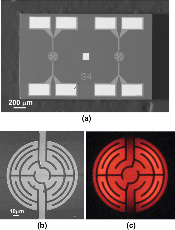
Preliminarily fabricated device. a SEM image of the twin micro-heater. b Large magnification of the active area. c Optical photo of the filament under operation. The filament power consumption was 40 mW
10 illustrates the structure of the preliminarily fabricated device used to determine the starting values of G and η for the design procedure. The active area diameter was 150 μm. The membrane structure and size were similar to that of the designed microheater described in the main text.
-
(ii)
Determination procedure of G(ΔT) value

For example, in this section authors describe the method which was used to calculate the total surface thermal loss coefficient of the designed microheater. We note, the G(475) value (see Table 1 in the main text) was approximated in a similar manner for the preliminarily fabricated device too using its own filament dimensions and material constants.
To calculate the G experimentally, we use the measured dimensions of the inner segments and inner filament rings, the average temperature of the filaments rings, heater current values and filament material constants. We note, due to the etching process, these measured dimensions show a few micron deviation compared to the targeted size. Based on these values the electric power dissipation for each inner ring can be calculated. Dividing the electric power value with the segment area we get the individual Gi values for every inner segment. The average of these Gi values results the total surface thermal loss coefficient G(ΔT) at the given active area temperature.
Using the filament material constants in Table 1, the measured filament dimensions of a realised device, and the heater current at 500 °C, the G(ΔT) values were calculated for the two inner filament rings. The area of the first segment was found to A1 = 7606μm2, the filament power consumption of the first segment was c.c. PE1 = 3.52mW, calculated by Eq. (32). Applying Eq. (5) to the first segment its total surface thermal loss coefficient is G1(475 °C) = PE1/A1 = 462 × 10−9 W/μm2. This value for the second segment was G2(475 °C) = PE2/A2 = 438 × 10−9 W/μm2. The mean value of these former two G values is G(475 °C) = 450 × 10−9 W/μm2 ± 2.6%. We note, the difference between the calculated G1 and G2 values is low, but due to the accuracy of the filament size measurement method and line width deviations the relative error of the calculated G (ΔT) value is around 10–15%.
Rights and permissions
Open Access This article is licensed under a Creative Commons Attribution 4.0 International License, which permits use, sharing, adaptation, distribution and reproduction in any medium or format, as long as you give appropriate credit to the original author(s) and the source, provide a link to the Creative Commons licence, and indicate if changes were made. The images or other third party material in this article are included in the article's Creative Commons licence, unless indicated otherwise in a credit line to the material. If material is not included in the article's Creative Commons licence and your intended use is not permitted by statutory regulation or exceeds the permitted use, you will need to obtain permission directly from the copyright holder. To view a copy of this licence, visit http://creativecommons.org/licenses/by/4.0/.
About this article

Cite this article
Bíró, F., Deák, A., Bársony, I. et al. An analytical method to design annular microfilaments with uniform temperature. Microsyst Technol 28, 2511–2528 (2022). https://doi.org/10.1007/s00542-022-05376-8
Received:
Accepted:
Published:
Issue Date:
DOI: https://doi.org/10.1007/s00542-022-05376-8