Photoluminescence of (Zn, Pb, Mn)S Quantum Dots in Polyacrylate Matrix A. A. IsaevaV. P. Smagin SEMICONDUCTOR STRUCTURES, LOW-DIMENSIONAL SYSTEMS, AND QUANTUM PHENOMENA 09 May 2020 Pages: 511 - 517
Prediction of the Magnitude of the Trapped Charge in the Buried Oxide of Silicon-on-Insulator Structures Using the Poole–Frenkel Effect A. A. ShiryaevV. M. VorotyntsevE. L. Shobolov SEMICONDUCTOR STRUCTURES, LOW-DIMENSIONAL SYSTEMS, AND QUANTUM PHENOMENA 09 May 2020 Pages: 518 - 522
Low-Dimensional Silicon-Carbide Structures: Analytical Estimates of Electron-Spectrum Characteristics S. Yu. Davydov SEMICONDUCTOR STRUCTURES, LOW-DIMENSIONAL SYSTEMS, AND QUANTUM PHENOMENA 09 May 2020 Pages: 523 - 528
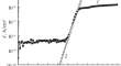
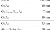
Carrier-Transport Processes in n+-GaAs/n0-GaAs/n+-GaAs Isotype Heterostructures with a Thin Wide-Gap AlGaAs Barrier S. O. SlipchenkoA. A. PodoskinN. A. Pikhtin SEMICONDUCTOR STRUCTURES, LOW-DIMENSIONAL SYSTEMS, AND QUANTUM PHENOMENA 09 May 2020 Pages: 529 - 533
Effect of Annealing on the Dark and Illuminated I(V ) Characterization of a ZnO:Ga|Cu2O Hetero-Junction Prepared by Ultrasonic Spray System H. TrirL. RadjehiN. Attaf SEMICONDUCTOR STRUCTURES, LOW-DIMENSIONAL SYSTEMS, AND QUANTUM PHENOMENA 09 May 2020 Pages: 534 - 542
Interfacial Characterization and Transport Conduction Mechanisms in Al|HfO2|p-Ge Structures: Energy Band Diagram M. A. BotzakakiG. SkoulatakisC. A. Krontiras SEMICONDUCTOR STRUCTURES, LOW-DIMENSIONAL SYSTEMS, AND QUANTUM PHENOMENA 09 May 2020 Pages: 543 - 553
Effects of 1-MeV Electron Irradiation on the Photoluminescence of GaInNAs|GaAs Single Quantum Well Structure M. SailaiA. AierkenG. Qi SEMICONDUCTOR STRUCTURES, LOW-DIMENSIONAL SYSTEMS, AND QUANTUM PHENOMENA 09 May 2020 Pages: 554 - 557
Polarization Processes in Thin Layers of Amorphous MoS2 Obtained by RF Magnetron Sputtering A. A. KononovR. A. Castro-ArataA. V. Kolobov AMORPHOUS, VITREOUS, AND ORGANIC SEMICONDUCTORS 09 May 2020 Pages: 558 - 562
Effect of Uniaxial Elastic Deformation on the Current–Voltage Characteristic of Surface-Barrier Sb–p-Si〈Mn〉–Au Diodes O. O. MamatkarimovO. KhimmatkulovI. G. Tursunov PHYSICS OF SEMICONDUCTOR DEVICES 09 May 2020 Pages: 563 - 566
S-Shaped I–V Characteristics of High-Power Schottky Diodes at High Current Densities A. G. TandoevT. T. MnatsakanovS. N. Yurkov PHYSICS OF SEMICONDUCTOR DEVICES 09 May 2020 Pages: 567 - 574
Modeling the Spatial Switch-On Dynamics of a Laser Thyristor (λ = 905 nm) Based on an AlGaAs/InGaAs/GaAs Multi-Junction Heterostructure O. S. SobolevaV. S. GolovinA. A. Podoskin PHYSICS OF SEMICONDUCTOR DEVICES 09 May 2020 Pages: 575 - 580
Switching Control Model of Closed-Mode Structures in Large Rectangular Cavities Based on AlGaAs/InGaAs/GaAs Laser Heterostructures A. A. PodoskinD. N. RomanovichN. A. Pikhtin PHYSICS OF SEMICONDUCTOR DEVICES 09 May 2020 Pages: 581 - 586
A Novel 4H-SiC Super Junction UMOSFET with Hetero-Junction Diode for Enhanced Reverse Recovery Characteristics and Low Switching Loss J. KimK. Kim PHYSICS OF SEMICONDUCTOR DEVICES 09 May 2020 Pages: 587 - 595
Influence of a Nanoporous Silicon Layer on the Practical Implementation and Specific Features of the Epitaxial Growth of GaN Layers on SiC/por-Si/c-Si Templates P. V. SeredinD. L. GoloshchapovS. A. Kukushkin FABRICATION, TREATMENT, AND TESTING OF MATERIALS AND STRUCTURES 09 May 2020 Pages: 596 - 608
Formation of Multilayer Structures with Integrated Membranes Based on Porous Silicon V. V. BolotovK. E. IvlevV. E. Roslikov FABRICATION, TREATMENT, AND TESTING OF MATERIALS AND STRUCTURES 09 May 2020 Pages: 609 - 613