Influence of Deposition Conditions and Ion-Plasma Treatment of Thin Cobalt Films on Their Electrical Resistivity I. I. AmirovR. V. SelyukovE. S. Gorlachev OriginalPaper 19 February 2021 Pages: 1 - 7
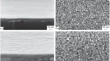
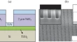
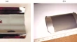
Metallization of Vias in Silicon Wafers to Produce Three-Dimensional Microstructures A. I. VorobjovaV. A. LabunovD. V. Grapov OriginalPaper 19 February 2021 Pages: 8 - 18
Influence of Resist Spreading during Its Dry Electron-Beam Etching on a Lateral Resolution A. G. IsaevF. A. SidorovA. E. Rogozhin OriginalPaper 19 February 2021 Pages: 19 - 23
Kinetics of the Volumetric and Heterogeneous Processes in the Plasma of a C4F8 + O2 + Ar Mixture A. M. EfremovD. B. MurinK.-H. Kwon OriginalPaper 19 February 2021 Pages: 24 - 32
Modification of Diazoquinone-Novolac Photoresist Films by the Implantation of Antimony Ions S. D. BrinkevichD. I. BrinkevichV. S. Prosolovich OriginalPaper 19 February 2021 Pages: 33 - 38
Effect of a Mixture’s Composition on the Electrophysical Parameters and Emission Spectra of Hydrogen Chloride Plasma with Chlorine and Helium S. A. PivovarenokD. B. MurinD. V. Sitanov OriginalPaper 19 February 2021 Pages: 39 - 44
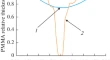
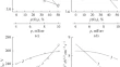
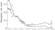
Experimental Study of the Influence of the Porosity of Thin-Film Silicon-Based Anodes on Their Charge-Discharge Characteristics T. L. KulovaL. A. MazaletskiiI. S. Fedorov OriginalPaper 19 February 2021 Pages: 45 - 53
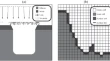
Numerical Simulation of Cryogenic Etching: Model with Delayed Desorption M. K. RudenkoA. V. Myakon’kikhV. F. Lukichev OriginalPaper 19 February 2021 Pages: 54 - 62
Effect of Process-Related Impurities on the Electrophysical Parameters of a MOS Transistor V. B. OdzhaevA. N. PetlitskiiYu. N. Yankovskii OriginalPaper 19 February 2021 Pages: 63 - 68
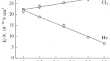
Domain Wall Precession in a Narrow Magnetic Nanowire O. S. TrushinN. I. Barabanova OriginalPaper 19 February 2021 Pages: 69 - 73