
Nothing in life is to be feared, it is only to be understood. Now is the time to understand more, so that we may fear less.
—Marie Curie
You have full access to this open access chapter, Download chapter PDF
Keywords
- Skin effect
- Skin depth
- High-frequency resistance
- Low-frequency resistance
- AC resistance
- DC resistance
- Per-unit-length resistance
- Surface resistance
- Resistance vs. frequency
10.1 Skin Depth
Introduction and definitions of the term skin depth δ [m] (Fig. 10.1):
-
Conductors. The skin depth δ [m] is defined as the distance from the conductor surface where the current density has fallen (caused by the skin effect) to 37% = 1/e = 1/2.72 of the current density at the surface of the conductor J 0 [A/m2]. The current density J d [A/m2] at distance d [m] from the conductor surface is defined as [2]:
$$\displaystyle \begin{aligned} |J_d| = |J_0| \cdot e^{-\frac{d}{\delta}} \end{aligned} $$(10.1)Fig. 10.1 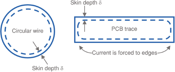
Skin depth δ
where:
-
|J d| = magnitude current density at distance d from the surface of the conductor in [A/m2]
-
|J 0| = magnitude of the current density at the surface of the conductor in [A/m2]
-
d = distance from the conductor’s surface in [m]
-
δ = skin depth in [m]
-
-
Shielding. Imagine an electromagnetic plane wave of field strength E 0 [V/m] and H 0 [A/m] entering an absorbing material (shield). The skin depth δ [m] is the distance an electromagnetic wave has to travel through that absorbing material until its field strength is reduced to 37% of E 0 or H 0 (Fig. 10.2). This means that the power of the plane electromagnetic wave is lowered by \(10 \log _{10}\left (1/e^2\right ) = {8.686}^{dB}\) after it has traveled the distance δ. The attenuation of an electromagnetic plane wave is defined like this [2]:
$$\displaystyle \begin{aligned} |E_d| &= \operatorname{Re}(|E_0| \cdot e^{-\underline{\gamma}d}) = \operatorname{Re}(|E_0| \cdot e^{-\alpha d} \cdot e^{-j \beta d}) = |E_0| \cdot e^{-\alpha d} = |E_0| \cdot e^{-\frac{d}{\delta}} {} \end{aligned} $$(10.2)$$\displaystyle \begin{aligned} |H_d| &= \operatorname{Re}(|H_0| \cdot e^{-\underline{\gamma}d}) = \operatorname{Re}(|H_0| \cdot e^{-\alpha d} \cdot e^{-j \beta d}) = |H_0| \cdot e^{-\alpha d} = |H_0| \cdot e^{-\frac{d}{\delta}} {} \end{aligned} $$(10.3)where:
-
|E 0| = electric field strength of an electromagnetic plane wave at the surface of a shield barrier, when entering that shield barrier in [V/m]
Fig. 10.2 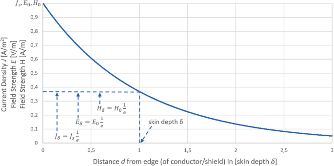
Attenuation of current density J [A/m2], electric field strength E [V/m], and magnetic field strength H [A/m] due to skin effect
-
|H 0| = magnetic field strength of an electromagnetic plane wave at the surface of a shield barrier, when entering that shield barrier in [A/m]
-
|E d| = electric field strength after the electromagnetic plane wave has traveled distance d through the shield barrier in [V/m]
-
|H d| = magnetic field strength after the electromagnetic plane wave has traveled distance d through the shield barrier in [A/m]
-
\( \underline {\gamma } =\) the complex propagation constant of the shield barrier material [1/m]
-
α = attenuation constant of the shield barrier material in [1/m]
-
β = phase constant (or phase factor) of the shield barrier material in [rad/m]
-
d = distance from the shield barrier’s surface in [m]
-
δ = skin depth in [m]
-


From Eqs. 10.2 and 10.3, we know that the skin depth δ [m] is defined as the inverse of the attenuation constant α [1/m] [1]:
where:
-
ω = 2πf = angular frequency of the signal in [rad/sec]
-
𝜖′ = real part of the complex permittivity (\( \underline {\epsilon } = \epsilon ' - j \epsilon ''\)) in [F/m]
-
𝜖″ = imaginary part of the complex permittivity (\( \underline {\epsilon } = \epsilon ' - j \epsilon ''\)) in [F/m]
-
μ′ = real part of the complex permeability (\( \underline {\mu } = \mu ' - j \mu ''\)) in [H/m]
-
μ″ = imaginary part of the complex permeability (\( \underline {\mu } = \mu ' - j \mu ''\)) in [H/m]
For good conductors (with σ ≫ ω𝜖′ and \(\epsilon _r^{\prime } = 1.0\)) with negligible magnetic losses (μ″ = 0), we can write [2]:
where:
-
δ = skin depth in [m]
-
ω = 2πf = angular frequency of the signal in [rad/sec]
-
\(\mu _r^{\prime } =\) relative permeability of the material through which the signal current is flowing or through which the electromagnetic wave is traveling in [1]
-
μ 0 = 4π ⋅ 10−1 H/m = 12.57 ⋅ 10−7 H/m = permeability of vacuum
-
σ = specific conductance of the material through which the signal current is flowing or through which the electromagnetic wave is traveling in [S/m]
Figure 10.3 presents some example values of skin depths for silver, copper, gold, aluminum, nickel, iron, and stainless steel 316. The following points have to be considered when calculating the skin depth for ferromagnetic metals (like nickel, iron):
-
The relative permeability \( \underline {\mu }_r\) depends on the specific material and alloy.
Fig. 10.3 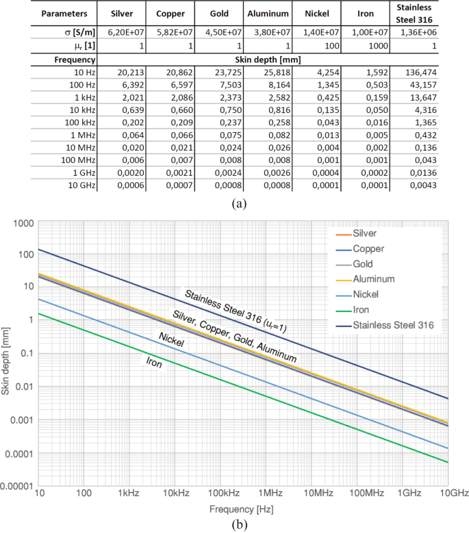
Skin depth of some example metals. Permeability \(\mu _r^{\prime }\) is assumed to be constant. (a) Table with the assumed electrical conductivity σ and permeability \(\mu _r^{\prime }\). (b) Skin depth δ as a function of frequency f
-
Relative permeability \( \underline {\mu }_r\) depends on the frequency f [Hz] and temperature T [K].

10.2 DC vs. AC Resistance
The resistance per-unit-length [Ω/m] for direct current (\(R_{DC}^{\prime }\)) and for alternating current (\(R_{AC}^{\prime }\)) of any conductor can be written as [2]:
where:
-
ρ = specific electrical resistivity of the conductor material in [Ωm]
-
σ = specific conductance of the conductor material in [S/m]
-
A = cross-sectional area of the conductor in [m2]
-
A eff = effective cross-sectional area of the conductor through which the current effectively flows in [m2]
For direct current (DC, 0 Hz), the cross-sectional area A eff [m2] through which the DC current flows is equal to the conductor cross-sectional area A [m2]. However, for high-frequency AC current with frequency f [Hz], the magnetic field—produced by current in the conductor—forces the current flow toward the outer surface of the conductor, and as a consequence of that, the current density increases exponentially from the core of the conductor toward the conductor’s surface. The higher the signal frequency f [Hz], the smaller the cross section A eff [m2] through which the current effectively flows.
The accurate calculation of A eff [m2] is difficult but can be reasonably approximated by assuming that the current is uniformly distributed over the skin depth δ [m]. In case of D ≫ δ, the approximate A effWire [m2] of a round conductor (circular wire) with diameter D [m] can be calculated as follows:
where:
-
A = cross-sectional area of the round conductor with diameter D in [m2]
-
A noCurr = the approximate cross-sectional area of the conductor where no current flows (as a consequence of the skin effect) in [m2]
-
δ = skin depth in [m]
-
D = diameter of round conductor in [m]
For a PCB trace according to Fig. 10.4, the effective area A effPCBtrace [m2] can be approximately calculated like this:
where:
-
A = cross-sectional area of the PCB trace with width w and height h in [m2]
Fig. 10.4 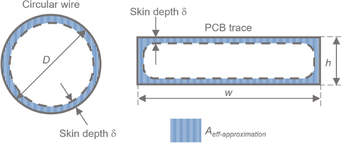
Approximation of A eff using the skin depth δ
-
A noCurr = the approximate cross-sectional area of the conductor where no current flows (as a consequence of the skin effect) in [m2]
-
δ = skin depth in [m]
-
w = width of the PCB trace in [m]
-
h = height or thickness of the PCB trace in [m]

Figure 10.5 shows \(R_{AC}^{\prime }\) [Ω/m] of a PCB trace versus a round copper wire. The calculations for \(R_{AC}^{\prime }\) [Ω/m] are approximations and ignore the return current path (proximity effect) and assume a single conductor surrounded by air only. However, the diagram gives an idea of how the skin effect influences the resistance at higher frequencies.

Increased resistance due to skin effect: PCB copper trace (width w = 0.25 mm, height h = 35 µm = 1 oz) vs. round copper wire (diameter D = 1 mm)
10.3 Surface Resistance
The surface resistance (or sheet resistance ) R s [Ω/square] for a thin layer with height h [m]—like shown in Fig. 10.6—is defined as [4]:
where:
-
σ = specific conductance of the conductor material in [S/m]
Fig. 10.6 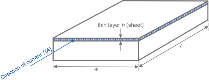
Sheet (thin layer) of height of h, width w, and length l. Current flow is parallel to length l (not perpendicular to the sheet)
-
h = height or thickness of a thin conductor layer [m]

For a good conductor (σ ≫ ω𝜖′), with negligible magnetic losses μ″ = 0 and at high frequency (skin depth δ much smaller than conductor cross-sectional dimensions), the thickness of the conductor sheet h [m] can be set to the skin depth δ [m], and the surface resistance R s [Ω/square] is defined as [3]:
where:
-
σ = specific conductance of the conductor material in [S/m]
-
δ = skin depth in [m]
-
ω = 2πf = angular frequency of the signal in [rad/sec]
-
\(\mu ' = \mu _r^{\prime } \mu _0 =\) ability to store energy in a medium when an external magnetic field is applied = real part of the complex permeability (\( \underline {\mu } = \mu ' - j \mu ''\)) in [H/m]
At high frequencies, where the current flows at the surface of the conductor (skin effect), the resistance of a conductor with perimeter p [m] and length l [m] can be approximated as:
where:
-
R s = surface resistance of the conductor material in [Ω/square]
-
l = length of the conductor in [m]
-
p = perimeter of the conductor in [m]
-
δ = skin depth in [m]
10.4 Summary
-
Skin Depth δ of Good Conductor.
$$\displaystyle \begin{aligned} \delta = \frac{1}{\sqrt{\pi f \mu_r^{\prime} \mu_0 \sigma}} \end{aligned} $$(10.13)where:
-
\(\mu _r^{\prime } =\) relative permeability of the conductor material in [1]
-
μ 0 = 4π ⋅ 10−1 H/m = 12.57 ⋅ 10−7 H/m = permeability of vacuum
-
σ = specific conductance of the conductor material in [S/m]
-
-
Resistance vs. Frequency. Due to the skin effect, the resistance of a conductor increases with increasing frequency. As an approximation and in case the skin depth δ [m] is much smaller than the conductor’s outer dimensions, it can be assumed that the current is uniformly distributed over the skin depth δ.
-
Surface Resistance. Surface resistance R s [Ω/square] of a good conductor at high frequency (skin depth δ much smaller than conductor cross-sectional dimensions):
$$\displaystyle \begin{aligned} R_s = \frac{1}{\sigma \delta} = \sqrt{\frac{\omega \mu'}{2 \sigma}} \end{aligned} $$(10.14)where:
-
σ = specific conductance of the conductor material in [S/m]
-
δ = skin depth in [m]
-
ω = 2πf = angular frequency of the signal in [rad/sec]
-
\(\mu ' = \mu _r^{\prime } \mu _0 =\) ability to store energy in a medium when an external magnetic field is applied = real part of the complex permeability (\( \underline {\mu } = \mu ' - j \mu ''\)) in [H/m]
-
References
Arthur von Hippel. Dielectrics and Waves. Artech House, 1954.
Clayton R. Paul. Introduction to electromagnetic compatibility. 2nd edition. John Wiley & Sons Inc., 2008.
David M. Pozar. Microwave engineering. 4th edition. Newens, 2012.
Brian C. Wadell. Transmission line design handbook. Artech House Inc., 1991.
Author information
Authors and Affiliations
Rights and permissions
Open Access This chapter is licensed under the terms of the Creative Commons Attribution 4.0 International License (http://creativecommons.org/licenses/by/4.0/), which permits use, sharing, adaptation, distribution and reproduction in any medium or format, as long as you give appropriate credit to the original author(s) and the source, provide a link to the Creative Commons license and indicate if changes were made.
The images or other third party material in this chapter are included in the chapter's Creative Commons license, unless indicated otherwise in a credit line to the material. If material is not included in the chapter's Creative Commons license and your intended use is not permitted by statutory regulation or exceeds the permitted use, you will need to obtain permission directly from the copyright holder.
Copyright information
© 2023 The Author(s)
About this chapter

Cite this chapter
Keller, R.B. (2023). Skin Effect. In: Design for Electromagnetic Compatibility--In a Nutshell. Springer, Cham. https://doi.org/10.1007/978-3-031-14186-7_10
Download citation
DOI: https://doi.org/10.1007/978-3-031-14186-7_10
Published:
Publisher Name: Springer, Cham
Print ISBN: 978-3-031-14185-0
Online ISBN: 978-3-031-14186-7
eBook Packages: EngineeringEngineering (R0)