
Abstract
In this chapter, we will present the interface between the physical environment and information processing (the cyphy-interface) together with the hardware required for processing, storing, and communicating information. Due to considering CPS, covering the cyphy-interface is indispensable. The need to cover other hardware components as well is a consequence of their impact on the performance, timing characteristics, power consumption, safety, and security.
You have full access to this open access chapter, Download chapter PDF
In this chapter, we will present the interface between the physical environment and information processing (the cyphy-interface) together with the hardware required for processing, storing, and communicating information. Due to considering CPS, covering the cyphy-interface is indispensable. The need to cover other hardware components as well is a consequence of their impact on the performance, timing characteristics, power consumption, safety, and security.
Regarding the cyphy-interface, we will present circuits for sampling and digitization of physical quantities as well as for the reverse process. We will present the sampling theorem and its impact. Regarding information processing, we will provide details of efficient hardware, in particular of digital signal processors, general-purpose computing on graphics processors, multi-core systems, and field programmable gate arrays (FPGAs). With respect to information storage, we will explain the memory hierarchy as it is used in embedded systems. We will also explain if and how existing communication technologies can be used.
Electronic information processing requires electrical energy. Accordingly, this chapter includes a section on the generation (e.g., harvesting), storage, and efficient use of electrical energy in embedded systems, including battery and energy consumption models. This chapter closes with a survey on the challenges of supporting security in hardware.
3.1 Introduction
Frequently, hardware designs are reused, either in the form of real hardware components or in the form of intellectual property (IP). The reuse of available hard- and software components is at the heart of the platform-based design methodology (see also p. 296). This methodology is seen as a key method for mastering the growing complexity of embedded systems. Consistent with the need to consider available hardware components and with the design information flow shown in Fig. 3.1, we are now going to describe some of the essentials of embedded system hardware.

Simplified design information flow
Hardware for embedded systems is much less standardized than hardware for personal computers. Due to the huge variety of embedded system hardware, it is impossible to provide a comprehensive overview of all types of hardware components. Nevertheless, we will try to provide a survey of some of the essential components which can be found in most systems. In many cyber-physical systems, especially in control systems, hardware is used in a loop (see Fig. 3.2). We will use this loop to structure the presentation of components in this chapter. In this (control) loop, information about the physical environment is made available through sensors. Typically, sensors generate continuous sequences of analog values. In this book, we will restrict ourselves to information processing where digital computers process discrete sequences of values. Appropriate conversions are performed by two kinds of circuits: sample-and-hold circuits and analog-to-digital converters (ADCs). After such conversion, information can be processed digitally. Generated results can be displayed and also be used to control the physical environment through actuators. Since many actuators are analog actuators, conversion from digital to analog signals may also be needed. We will see how this conversion can be achieved either by digital-to-analog converters (DACs) or indirectly by pulse-width modulation (PWM).

Hardware in the loop
Due to the prevailing electronic information processing, we assume that we require electrical energy. Some source of this energy must be available. If our energy source does not provide energy permanently, we may need to store energy, e.g., in rechargeable batteries or capacitors. During system operation, much of the electrical energy will be converted into thermal energy (heat). It may be necessary to remove thermal energy from the system.
This model is obviously appropriate for control applications. For other applications, it can be employed as a first-order approximation. In the following, we will describe essential hardware components of embedded and cyber-physical systems following the structure of Fig. 3.2.
3.2 Input: Interface Between Physical and Cyber-World
3.2.1 Sensors
Sensors are key components of the cyphy-interface. Sensors can be designed for virtually every physical quantity. There are sensors for weight, velocity, acceleration, electrical current, voltage, temperature, etc. A wide variety of physical effects can be exploited in the construction of sensors [151]. Examples include the law of induction (generation of voltages in an electric field) and photoelectric effects. There are also sensors for chemical substances [152].
Recent years have seen the design of a huge range of sensors, and much of the progress in designing smart systems can be attributed to modern sensor technology. The availability of sensors has enabled the design of sensor networks (see, e.g., Tiwari et al. [543]), a key element of the Internet of Things. It is impossible to cover this subset of cyber-physical hardware technology comprehensively, and we can only give characteristic examples:
-
Acceleration sensors: Figure 3.3 shows a small sensor manufactured using microsystem technology. The sensor contains a small mass in its center. When accelerated, the mass will be displaced from its standard position, thereby changing the resistance of the tiny wires connected to the mass.
Fig. 3.3 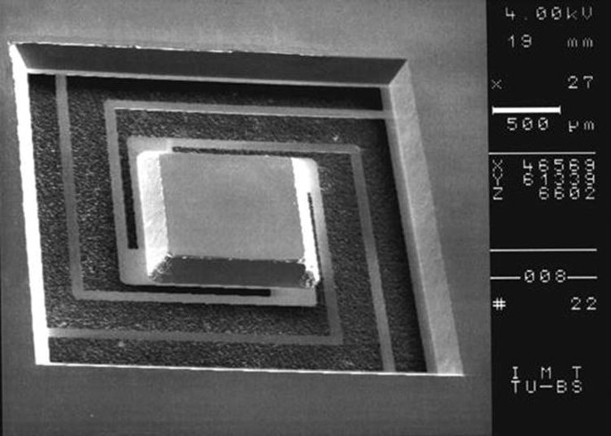
Acceleration sensor (courtesy S. Büttgenbach, IMT, TU Braunschweig), ⒸTU Braunschweig, Germany
Acceleration sensors are included in the powerful inertial measurement units (IMUs) (see, e.g., Siciliano et al. [487], Section 20.4). They contain gyros and accelerometers, and they capture up to six degrees of freedom, comprising position (x, y, and z) and orientation (roll, pitch, and yaw) [575]. They are contained in airplanes, cars, robots, and other products in order to provide inertial navigation.
-
Image sensors: There are essentially two kinds of image sensors: charge-coupled devices (CCDs) and CMOS sensors. In both cases, arrays of light sensors are used. The architecture of CMOS sensor arrays is similar to that of standard memories: individual pixels can be randomly addressed and read out. CMOS sensors use standard CMOS technology for integrated circuits. Due to this, sensors and logic circuits can be integrated on the same chip. This allows some preprocessing to be done already on the sensor chip, leading to so-called smart sensors. CMOS sensors require only a single standard supply voltage and interfacing in general is easy. Therefore, CMOS-based sensors can be cheap.
In contrast, CCD technology is optimized for optical applications. In CCD technology, charges must be transferred from one pixel to the next until they can finally be read out at an array boundary. This sequential charge transfer also gave CCDs their name. For CCD sensors, interfacing is more complex.
Selecting the most appropriate image sensor depends on several constraints, which change as technology evolves. The image quality of CMOS sensors has been improved over the recent years, and the initial image superiority of CCDs became questionable. Therefore, achieving a good image quality is feasible with CCD and with CMOS sensors. Due to their faster readout speed, CMOS sensors are preferred for cameras with live view modes or video recording functionality [404]. Also, CMOS sensors are preferred for low-cost devices and if smart sensors are to be designed. Several application areas for CCDs have disappeared, but they are still used in areas such as scientific image acquisition.
-
Biometric sensors: Demands for higher security standards as well as the need to protect mobile and removable equipment have led to an increased interest in authentication. Due to the limitations of password-based security (e.g., stolen and lost passwords), biometric sensors and biomedical authentication receive attention. Biometric authentication tries to identify whether or not a certain person is actually the person she or he claims to be. Methods for biometric authentication include iris scans, fingerprint sensors, and face recognition. False accepts as well as false rejects are an inherent problem of biometric authentication (see definitions on p. 257). In contrast to password-based authentication, exact matches are not possible.
-
Artificial eyes: Artificial eye projects have received significant attention. Some projects have an impact on the eye, but others provide vision in an indirect way. For example, the Dobelle Institute experimented with a camera attached to a computer sending electrical pulses to a direct brain contact [532]. More recently, the less invasive translation of images into audio has been preferred.
-
Radio frequency identification (RFID): RFID technology is based on the response of a tag to radio frequency signals [226]. The tag consists of an integrated circuit and an antenna, and it provides its identification to RFID readers. The maximum distance between tags and readers depends on the type of the tag. The technology is used to identify objects, animals, or people and is a key enabler for the Internet of Things.
-
Automotive sensors: Today’s cars contain a large number of sensors. This includes rain sensors, tire pressure sensors, collision sensors, etc. The overall goal is to provide comfort and safety to the passengers and the environment.
-
Other sensors: Other common sensors include thermal sensors, engine control sensors, Hall effect sensors, and many more.

Machine learning algorithms [188, 204, 453, 560] may need to be used to obtain meaningful information from noisy sensor readouts.
Sensors are generating signals. Mathematically, the following definition applies:
Definition 3.1
A signal σ is a mapping from a time domain D T to a value domain D V:
Signals may be defined over a continuous or a discrete time domain as well as over a continuous or a discrete value domain.
3.2.2 Discretization of Time: Sample-and-Hold Circuits
All known digital computers work in a discrete time domain D T. This means that they can process discrete sequences or streams of values. Hence, incoming signals over the continuous time domain must be converted to signals over the discrete time domain. This is the purpose of sample-and-hold circuits. These are included in the cyphy-interface. Figure 3.4 (left) shows a simple sample-and-hold circuit. In essence, the circuit consists of a clocked transistor and a capacitor. The transistor operates like a switch. Each time the switch is closed by the clock signal, the capacitor is charged so that its voltage h(t) is practically the same as the incoming voltage e(t). After opening the switch again, this voltage will remain essentially unchanged until the switch is closed again. Each of the values stored on the capacitor can be considered as an element of a discrete sequence of values h(t), generated from a continuous function e(t) (see Fig. 3.4 (right)). If we sample e(t) at times {t s}, then h(t) will be defined only at those times.

Sample-and-hold phase: left, circuit; right, signals
An ideal sample-and-hold circuit would be able to change the voltage at the capacitor in an arbitrarily short amount of time. This way, the input voltage at a particular instance in time could be transferred to the capacitor, and each element in the discrete sequence would correspond to the input voltage at a particular point in time. In practice, however, the transistor has to be kept closed for a short time window in order to really charge or discharge the capacitor. The voltage stored on the capacitor will then correspond to a voltage reflecting that short time window.
3.2.3 Fourier Approximation of Signals
Would we be able to reconstruct the original signal e(t) from the sampled signal h(t)? In order to answer this question, we revert to the fact that arbitrary signals can be approximated by summing (possibly phase-shifted) sine functions of different frequencies (Fourier approximation).Footnote 1
Example 3.1
A square wave can be approximated by Eq. (3.1) [440]:
In this equation, T is the period and approximation is improved for increasing K. Figures 3.5 and 3.6 visualize Eq. (3.1).

Approximation of a square wave by sine waves for K = 1 (left) and K = 3 (right)

Approximation of a square wave by sine waves for K = 7 (left) and K = 11 (right)
The larger difference between the square wave and its approximation at the jump discontinuities of the square wave (best visible for K=11) is called Gibbs phenomenon [440]. ∇
Definition 3.2
A signal transformation Tr is linear if for all signals e 1(t) and e 2(t) we have
Next, we restrict ourselves to linear systems. Then, in order to answer the question raised above, we study sampling each of the sine waves independently.
Example 3.2
Consider signals described by either of the two functions e 3 or e 4:
The sine waves used in these functions have periods of T = 8, 4, and 1, respectively (this can be seen by comparing these sine waves with those of Eq. (3.1)). A graphical representation of these functions is shown in Fig. 3.7. Suppose that we will be sampling these signals at integer times. It then so happens that both signals have the same value whenever they are sampled. Obviously, it is not possible to distinguish between e 3(t) and e 4(t) if we sample at these instances in time and if only the sampled signal is available. ∇

Visualization of functions e 3(t) (blue) and e 4(t) (red)
In general, sampled signals will not allow us to distinguish between some slow signal e 3(t) and some other faster varying signal e 4(t) if e 3(t) and e 4(t) are identical each time we are sampling the signals. The fact that two or more unsampled signals can have the same sampled representation is called aliasing. We are not sampling e 4(t) frequently enough to notice, for example, that it has slope changes between integer times. So, from this counterexample we can conclude that reconstruction of the original unsampled signal is not feasible unless we have additional knowledge about the frequencies or the waveforms present in the input signal.
How frequently do we have to sample signals to be able to distinguish between different sine waves? Let us assume that we are sampling the input signal at constant time intervals, such that T s is the sampling period:
Let
be the sampling rate or sampling frequency. Then, sampling theory provides us with the following theorem (see, e.g., [440]):
Theorem 3.1 (Sampling Theorem)
Given the above definitions of variables, aliasing is avoided if we restrict the frequencies of the incoming signal to less than half of the sampling frequency f s:
Definition 3.3
f N is called the Nyquist frequency; f s is the sampling rate.
The condition in Eq. (3.8) is called sampling criterion, and sometimes the Nyquist sampling criterion.
Therefore, reconstruction of input signals e(t) from discrete samples h(t) can be successful only if we make sure that higher-frequency components such as the one in e 4(t) are removed. This is the purpose of anti-aliasing filters. Anti-aliasing filters are placed in front of the sample-and-hold circuit (see Fig. 3.8).

Anti-aliasing placed in front of the sample-and-hold circuit
Figure 3.9 demonstrates the ratio between the amplitudes of the output and the input waves as a function of the frequency for this filter. Ideally, such a filter would remove all frequencies at and above half the sampling frequency and keep all other components unchanged. This way, it would convert signal e 4(t) into signal e 3(t).

Ideal and realizable anti-aliasing filters (low-pass filters)
In practice, such ideal filters (so-called brick-wall filters) do not exist.Footnote 2 Realizable filters will already start attenuating frequencies smaller than f s∕2 and will still not eliminate all frequencies larger than f s∕2 (see Fig. 3.9). Attenuated high-frequency components will exist even after filtering. For frequencies smaller than f s∕2, there may also be some “overshooting,” i.e., frequencies for which there is some amplification of the input signal.
The design of good anti-aliasing filters is an art by itself. This art has been studied, for example, in great detail for high-quality audio equipment, involving detailed hearing tests. Many of the perceived differences between high-quality equipment have been attributed to the design of such filters.
3.2.4 Discretization of Values: Analog-to-Digital Converters
Since we are restricting ourselves to digital computers, we must also replace signals that map time to a continuous value domain D V by signals that map time to a discrete value domain \(D^{\prime }_V\). This conversion from analog-to-digital values is done by analog-to-digital converters (ADCs). There is a large range of ADCs with varying speed/precision characteristics. Typically, fast ADCs have a low precision and high-precision converters are slow.
We will present several converters in the next subsections.
3.2.4.1 Flash ADC
This type of ADCs uses a large number of comparators. Each comparator has two inputs, denoted as + and -. If the voltage at input + exceeds that at input -, the output corresponds to a logical ’1’, and it corresponds to a logical ’0’ otherwise.Footnote 3
In the ADC, all - inputs are connected to a voltage divider. If input voltage h(t) exceeds \(\frac {3}{4} V_{ref}\), the comparator at the top of Fig. 3.10 (left) will generate a ’1’. The encoder at the output of the comparators will try to identify the most significant ’1’ and will encode this case as the largest output value. The case h(t) > V ref should normally be avoided since V ref is typically close to the supply voltage of the circuit and input voltages exceeding the supply voltage can lead to electrical problems. In our case, input voltages larger than V ref generate the largest digital value as long as the converter does not fail due to the high input voltage.

Flash ADC: left, schematic; right, w as a function of h
Now, if input voltage h(t) is less than \(\frac {3}{4} V_{ref}\), but still larger than \(\frac {2}{4} V_{ref}\), the comparator at the top of Fig. 3.10 will generate a ’0’, while the next comparator will still signal a ’1’. The encoder will encode this as the second largest value.
Similar arguments hold for cases \(\frac {1}{4} V_{ref} < h(t) < \frac {2}{4} V_{ref}\) and \(0 < h(t) < \frac {1}{4} V_{ref}\), which will be encoded as the third largest and the smallest value, respectively. Figure 3.10 (right) shows the relation between input voltages and generated digital values.
The outputs of the comparators encode numbers in a special way: if a certain comparator output is equal to ’1’, then all the less significant outputs are all equal to ’1’. The encoder transforms this representation of numbers into the usual representation of natural numbers. The encoder is actually a so-called priority encoder, encoding the most significant input number carrying a ’1’ in binary.Footnote 4
The circuit can convert positive analog input voltages into digital values. Converting both positive and negative voltages and generating two’s complement numbers requires some extensions. One nice property of the flash ADC is the fact that it is automatically monotonic: For any increase in the analog voltage from 0 to the maximum, the corresponding digital value increases as well. This property is maintained even if the actual value of the resistors would deviate from the nominal value. However, such a deviation would have an impact on the precision of the linear relation expected between analog and digital values.
Unfortunately, the chain of resistors forms a conducting path, which exists even if the converter is not used. This could make it impossible to use this converter for low-power equipment.
In general, ADCs are also characterized by their resolution. This term has several different but related meanings [15]. The resolution (measured in bits) is the number of bits produced by an ADC. For example, ADCs with a resolution of 16 bits are needed for many audio applications. However, the resolution is also measured in volts, and in this case it denotes the difference between two input voltages causing the output to be incremented by 1:

Example 3.3
For the ADC of Fig. 3.10, the resolution is 2 bits or \(\frac {1}{4} V_{ref}\) volts, if we assume V ref as the largest voltage. ∇
The key advantage of the flash ADC is its speed. It does not need any clock. The delay between the input and the output is very small, and the circuit can be used easily, for example, for high-speed video applications. The disadvantage is its hardware complexity: we need n − 1 comparators in order to distinguish between n values. Imagine using this circuit in generating digital audio signals for CD recorders. We would need 216 − 1 comparators! High-resolution ADCs must be built differently.
3.2.4.2 Successive Approximation
Distinguishing between a large number of digital values is possible with ADCs using successive approximation. The circuit is shown in Fig. 3.11.

Circuit using successive approximation
The key idea of this circuit is to use binary search. Initially, the most significant output bit of the successive approximation register is set to ’1’; all other bits are set to ’0’. This digital value is then converted to an analog value, corresponding to 0.5 ∗ the maximum input voltage.Footnote 5 If h(t) exceeds the generated analog value, the most significant bit is kept at ’1’; otherwise it is reset to ’0’.
This process is repeated with the next bit. It will remain set to ’1’ if the input value is either within the second or the fourth quarter of the input value range. The same procedure is repeated for all the other bits.
Figure 3.12 shows an example. Initially the most significant bit is set to ’1’. This value is kept, since the resulting V − is less than h(t). Then, the second most significant bit is set to ’1’. It is reset to ’0’, since the resulting V − is exceeding h(t). Next, the third most significant bit is tried. It is set to ’1’, and this value is kept. Finally, the least significant bit is also set, and it remains set after the comparison has been completed. Obviously, h(t) must be constant during the conversion, otherwise the whole procedure would be jeopardized. This requirement is met if we employ a sample-and-hold circuit as shown above. The resulting digital signal is called w(t).

Successive approximation
The key advantage of the successive approximation technique is its hardware efficiency. In order to distinguish between n digital values, we need \(\left \lceil log_2(n)\right \rceil \) bits in the successive approximation register and the D/A converter. The disadvantage is its speed, since it needs \(\mathcal {O}(log_2(n))\) steps. These converters can therefore be used for high-resolution applications, where moderate speeds are required. Examples include audio applications.
3.2.4.3 Pipelined Converters
These converters consist of a chain of converters, where each stage in the chain is in charge of converting a few bits (see Fig. 3.13). Each stage passes the remaining residue of the voltage to the next stage (if any). For example, each stage could convert a single bit and subtract the corresponding voltage. The resulting residue would typically be scaled up by a factor of two (in order to avoid too small voltages) and be passed on to the next stage. Typically, each stage would include a flash ADC of a few bits and a D/A converter to compute the voltage to be subtracted. Resulting digital values must be aligned in time. Required hardware resources increase linearly with the number of bits. With this structure, a good throughput can be achieved, but the latency is larger than for flash converters.

Pipelined ADC [291]
3.2.4.4 Other Converters
Integrating converters use (at least) two phases for the measurement. During the first phase of length t 1, the integral of the input voltage over time is computed.Footnote 6 For constant inputs, the resulting value V out is proportional to the input voltage (V out ∼ V in ∗ t 1). During the second phase, this value is decreased at a constant rate, and the time to reach a value of zero is counted. The final count is proportional to the input voltage. Hence, using proper scaling, the final count represents the input voltage. If the input voltage contains some noise, its impact is likely to be averaged out during the first integration phase. Hence, these converters are capable of compensating noise. They are typically found in slow, high-resolution multimeters.
For folding ADCs, the input voltage range is divided into 2m segments [100, 321]. A coarse-grained converter detects the segment of the current input voltage, yielding the m most significant output bits. A fine-grained converter computes the value within a segment, yielding the less significant output bits.
For delta-sigma ADCs (Δ Σ ADCs), the name indicates that signal differences (Δs) are encoded and that they are summed up (Σ). A description of these converters is beyond the scope of this book. For details refer to Khorramabadi [292].
3.2.4.5 Comparison of ADCs
Figure 3.14 provides an overview of the speed/resolution trade-offs of ADCs, using a trade-off analysis of Vogels et al. [558]. Flash ADCs are clearly the fastest but provide only a small resolution. Pipelining is frequently superior to successive approximation. Another overview of ADCs is provided by IEEE TV [437].

Comparison of the speed/resolution characteristics of various ADCs [558]
3.2.4.6 Quantization Noise
Figure 3.15 shows the behavior of a flash ADC when the input signal is that of Eq. (3.3). Only the behavior for a positive input signal is shown. The figure includes the voltage corresponding to the digital value, the original voltage, and the difference between the two. Obviously, the converter is “truncating” the digital representation of the analog signal to the number of available bits (i.e., the digital value is always less than or equal to the analog value). This is a consequence of the way in which the flash converter is doing comparisons. “Rounding” converters would need an internal correction by “half a bit.” Effectively, the digital signal encodes values corresponding to the sum of the original analog values and the difference w(t) − h(t). This means, it appears as if the difference between the two signals had been added to the original signal. This difference is a signal called quantization noise:

h(t) (blue), w(t) (red), w(t) − h(t) (black)
Definition 3.4
Let h(t) be some analog signal. Let w(t) be derived from h(t) by quantization. The difference between the two is called quantization noise:
Increasing the resolution of the ADC decreases quantization noise. The impact of quantization noise is captured in the definition of the signal-to-noise ratio (SNR) , measured in decibels (tenth of a bel, named after Alexander G. Bell).
Definition 3.5
The SNR is defined as follows:
We have used that, for any given impedance R, the power of a signal is proportional to the square of the voltage. Decibels are no physical units, since the SNR is dimensionless.
For any signal h(t), the power of the quantization noise is equal to α ∗ Q, where α ≤ 1 depends on the waveform of h(t). If h(t) can always be represented exactly by a digital value, then α = 0. If h(t) is always “just a little” below the next value that can be represented, α may be close to 1.
Example 3.4
The SNR of 16 bit CD audio is (for α ≈ 1) about 20 ∗ log(216) = 96 dB. Values of α < 1 and imperfect ADCs change this number. ∇
3.3 Processing Units
Let us now discuss the next hardware element in the loop of Fig. 3.2, processing units. For information processing in embedded systems, we will consider ASICs (application-specific integrated circuits) using hardwired multiplexed designs, reconfigurable logic, and programmable processors. We will consider ASICs first.
3.3.1 Application-Specific Integrated Circuits (ASICs)
For high-performance applications and for large markets, application-specific integrated circuits (ASICs) can be designed. In general, ASICs are very energy-efficient (see Sect. 3.7.3 on p. 67). However, the cost of designing and manufacturing such chips is quite high. The cost of the mask set (which is used for transferring geometrical patterns onto the chip) has grown.Footnote 7
It is feasible to decrease this cost by using less advanced semiconductor fabrication technologies and by using multi-project wafers (MPW) containing several designs. But there is a lack of flexibility: correcting design errors typically requires a new mask set and a new fabrication run (unless the ASIC contains processors with writable memories). This approach also has to cope with potentially large design efforts requiring dedicated skills and expensive tools. Therefore, ASICs are appropriate only under special circumstances, like large market volumes, ultimate energy efficiency demands, special voltage or temperature ranges, mixed analog/digital signals, or security-driven designs. Hence, the design of ASICs is not covered in this book.
3.3.2 Processors
The key advantage of processors is their flexibility. With processors, the behavior of embedded systems can be changed by changing the software running on those processors. Changes of the behavior may be required in order to correct design errors, to update the system to a new standard, or to add features. Because of this, processors have found widespread use in embedded systems. In particular, processors which are available commercially “off-the-shelf” (COTS) have become very popular.
Embedded processors must be used in a resource-aware manner, i.e., we need to care about resources required for running applications on them. Furthermore, they do not need to be instruction set compatible with commonly used personal computers (PCs) or servers. Therefore, their architectures may be different from those processors. Efficiency has different aspects (see p. 13), some of which are discussed next.
3.3.2.1 Energy Efficiency
The energy E for an application is related to the power P as a function of time, since
Let us assume that we start with some design having a power consumption of P 0(t), leading to an energy consumption of
after t 0 units of execution time. Suppose that a modified design finishing computations already at time t 1 comes with a power consumption of P 1(t) and an energy consumption of
If P 1(t) is not too much larger than P 0(t), then a reduction of the execution time also reduces the energy consumption. However, in general this is not necessarily always true. The situation is also shown in Fig. 3.16: E 1 may be smaller than E 0, but E 1 can also be larger than E 0. So, if the energy consumption is to be minimized, it should be used as a cost function. Just minimizing the execution time can be misleading.

Comparison of energies E 0 and E 1
Minimization of power and energy consumption are both important. Power consumption has an effect on the size of the power supply, the design of the voltage regulators, the dimensioning of the interconnect, and short-term cooling. Minimizing the energy consumption is required especially for mobile applications, since battery technology is only slowly improving and since the cost of energy may be quite high. Also, a reduced energy consumption decreases cooling requirements and improves the reliability (since the lifetime of electronic circuits decreases for high temperatures).
Next, we would like to demonstrate that for CMOS technology, it is preferable to replace high-speed sequential computations by reduced speed parallel computations. This is shown by—first of all—considering the power consumption of CMOS devices. The dynamic power consumption is the power consumption caused by switching (in contrast to the static power consumption which exists even if no switching takes place). The average dynamic power consumption P dyn of CMOS circuits is given by Chandrakasan et al. [90]
where α is the switching activity, C L is the load capacitance, V dd is the supply voltage, and f is the clock frequency. This means that the power consumption of CMOS processors increases (at least)Footnote 8 quadratically with the supply voltage V dd.
The delay of CMOS circuits can be approximated as [90]
where k is a constant and V t is the threshold voltage. V t has an impact on the transistor input voltage required to switch the transistor on. For example, for a maximum supply voltage of V dd,max = 3.3 V, V t may be in the order of 0.8 V. Consequently, the maximum clock frequency is a function of the supply voltage. However, decreasing the supply voltage reduces the power quadratically, while the run-time of algorithms is only linearly increased (ignoring the effects of the memory system).
We can use this to reduce the amount of energy required for a certain amount of computations. Let us assume that we are initially performing computations sequentially at voltage V dd, constant power P, clock frequency f, run-time of t, and energy consumption E = P ∗ t.
Now let us assume that we are moving toward executing β operations in parallel. Due to parallel execution, we can extend the time for each operation by a factor of β. In turn, we can also reduce frequency f by a factor of β and use a new frequency
This allows us to also reduce the voltage to a new voltage
This reduces the power P 0 per operation quadratically:
Due to executing β operations in parallel, the overall power P′ can be computed as
The time t′ to execute operations in parallel is the same as the time to compute them sequentially (t′ = t). Hence, the energy to execute the operations in parallel is
We conclude that it is more energy-efficient to execute β operations in parallel instead of computing them sequentially. However, our derivation contains a number of approximations. On the one hand, power may be depending even cubically on the voltage, and we have ignored the fact that memory speed is frequently a limiting constraint. Faster processor clock speeds might just lead to more waiting for memory accesses (but there may be also conflicts for memory access from multiple cores). The energy would decrease quadratically if we would be able to keep the power consumption independent of the level of parallelism. On the other hand, we need to be able to find β operations which can be executed in parallel. Overall, we keep in mind that parallel execution is a means for deriving energy-efficient implementations, regardless of which hardware technology we are using.
Architectures must be optimized for their energy efficiency, and we must make sure that we are not losing efficiency in the software generation process. For example, compilers generating 50% overhead in terms of the number of cycles will take us further away from the efficiency of ASICs, possibly by even more than 50%, if the supply voltage and the clock frequency must be increased in order to meet timing deadlines.
There is a large amount of techniques available that can make processors energy-efficient, and energy efficiency should be considered at various levels of abstraction, from the design of the instruction set down to the design of the chip manufacturing process [77]. Gated clocking and power gating are examples of such techniques. With gated clocking, parts of the processor are disconnected from the clock during idle periods. In a similar way, the power can be disconnected for some components. For example, direct memory access (DMA) hardware or bus bridges can be disconnected if they are not needed. Also, there are attempts, to get rid of the clock for major parts of the processor altogether. There are two contrasting approaches: globally synchronous locally asynchronous (GSLA) processors [436] and globally asynchronous locally synchronous (GALS) processors [262]. Further information about low-power design techniques is available in a book by E. Macii [359] and in the PATMOS proceedings (see http://www.patmos-conf.org/).
At least three techniques can be applied at a rather high level of abstraction:
-
Parallel execution: According to Eq. (3.20), parallel execution is an effective means of improving the overall energy efficiency.
-
Dynamic power management (DPM): With this approach, processors have several power-saving states in addition to the standard operating state. Each power-saving state has a different power consumption and a different time for transitions into the operating state. Figure 3.17 shows the three states for the StrongARM SA-1100 processor.
Fig. 3.17 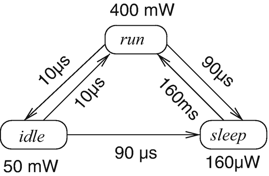
Dynamic power management states of the StrongARM SA-1100 processor [47]
The processor is fully operational in the run state. In the idle state, it is just monitoring the interrupt inputs. In the sleep state, on-chip activity is shut down, the processor is reset, and the chip’s power supply is shut off [593]. A separate I/O power supply provides power to power manager hardware. The processor can be restarted by the power manager hardware by a preprogrammed wake-up event. Note the large difference in the power consumption between the sleep state and the other states, and note also the large delay for transitions from the sleep to the run state.
-
Dynamic voltage and frequency scaling (DVFS): Equation (3.14) can be exploited in a technique called dynamic voltage and frequency scaling (DVFS). For example, the Crusoe™ processor by Transmeta [295] provided 32 voltage levels between 1.1 and 1.6 V, and the clock could be varied between 200 MHz and 700 MHz in increments of 33 MHz. Transitions from one voltage/frequency pair to the next took about 20 ms. Design issues for DVFS-capable processors are described in a paper by Burd and Brodersen [76]. In 2004, Intel SpeedStep ® Technology provided six different voltage/frequency combinations for Pentium™ M processors [246]. More recent processors include more comprehensive mechanisms for power management.

3.3.2.2 Code Size Efficiency
Minimizing the code size is very important for embedded systems, since large hard disk drives (HDDs) or solid-state disks (SSDs) are typically not available and since the capacity of memory is typically also very limited.Footnote 9 This is even more pronounced for systems on a chip (SoCs). For SoCs, the memory and processors are implemented on the same chip. In this particular case, memory is called embedded memory. Embedded memory may be more expensive to fabricate than separate memory chips, since the fabrication processes for memories and processors must be compatible. Nevertheless, a large percentage of the total chip area may be consumed by the memory. There are several techniques for improving the code size efficiency:
-
CISC machines: Standard RISC processors have been designed for speed, not for code size efficiency. Earlier complex instruction set processors (CISC machines) were actually designed for code size efficiency, since they had to be connected to slow memories. Caches were not frequently used. Therefore, “old-fashioned” CISC processors are finding applications in embedded systems. ColdFire processors [170], which are based on the Motorola 68000 family of CISC processors, are an example.
-
Compression techniques: In order to reduce the amount of silicon needed for storing instructions as well as in order to reduce the energy needed for fetching these instructions, instructions are stored in memory in compressed form. This reduces both the area and the energy necessary for fetching instructions. Due to the reduced bandwidth requirements, fetching can also be faster. A (hopefully small and fast) decoder is placed between the processor and the (instruction) memory in order to generate the original instructions on the fly (see Fig. 3.18 (right)).Footnote 10 Instead of using a potentially large memory of uncompressed instructions, we are storing the instructions in a compressed format.
Fig. 3.18 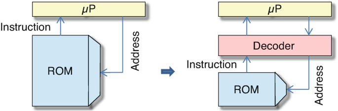
Schemes for instruction fetch: left, uncompressed; right, compressed
The goals of compression can be summarized as follows:
-
We would like to save ROM and RAM areas, since these may be more expensive than the processors themselves.
-
We would like to use some encoding technique for instructions and possibly also for data with the following properties:
-
⋅ There should be little or no run-time penalty for these techniques.
-
⋅ Decoding should work from a limited context (it is, e.g., impossible to read the entire program to find the destination of a branch instruction).
-
⋅ Word sizes of the memory, of instructions, and of addresses must be taken into account.
-
⋅ Branch instructions branching to arbitrary addresses must be supported.
-
⋅ Fast encoding is only required if writable data is encoded. Otherwise, fast decoding is sufficient.
-
There are several variations of this scheme:
-
For some processors, there is a second instruction set. This second instruction set has a narrower instruction format. An example of this is the ARM® processor family. The original ARM instruction set is a 32 bit instruction set. Most ARM processors also provide a second instruction set, with 16 bit wide instructions, called THUMB instructions. THUMB instructions are shorter, since they do not support predication,11 use shorter and less register fields, and use shorter immediate fields (see Fig. 3.19).
Fig. 3.19 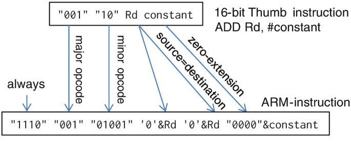
Re-encoding THUMB into ARM instructions
THUMB instructions are dynamically converted into ARM instructions while programs are decoded. THUMB instructions can use only half the registers in arithmetic instructions. Therefore, register fields of THUMB instructions are concatenated with a ’0’ bit.Footnote 12 In the THUMB instruction set, source and destination registers are identical, and the length of constants that can be used is reduced by 4 bits. During decoding, pipelining is used to keep the run-time penalty low.
Similar techniques also exist for other processors. The disadvantage of this approach is that the tools (compilers, assemblers, debuggers, etc.) must be extended to support a second instruction set. Therefore, this approach can be quite expensive in terms of software development cost.
-
A second approach is the use of dictionaries. With this approach, each instruction pattern is stored only once. For each value of the program counter, a look-up table provides a pointer to the corresponding instruction in the instruction table, the dictionary (see Fig. 3.20).
Fig. 3.20 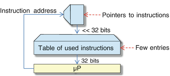
Dictionary approach for instruction compression
This approach relies on using only very few different instruction patterns. Therefore, only few entries are required for the instruction table. Hence, the bit width of the pointers can be quite small. Many variations of this scheme exist. Some are called two-level control store [118], nanoprogramming [514], or procedure ex-lining [551].
Beszedes [52] and Latendresse [324] provide overviews of a large number of known compression techniques. In addition, Bonny et al. [58] published a Huffman-based technique.
-


3.3.2.3 Execution Time Efficiency Using Digital Signal Processing as an Example
In order to meet time constraints without having to use high clock frequencies, architectures can be customized to certain application domains, such as digital signal processing (DSP). Let us have a closer look at DSP now! In digital signal processing, digital filtering is a very frequent operation. Let us assume that we are extending the pipeline of Fig. 3.8 on p. 9. We add a processing component, supposed to perform filtering. Names of signals are shown in Fig. 3.21.

Naming conventions for signals
Equation (3.21) describes a digital filter generating an output signal x(t) from an input signal w(t). Both signals are defined over the (usually unbounded) domain {t s} of sampling instances. We write x s instead of x(t s) and w s−n+k+1 instead of w(t s−n+k+1):Footnote 13
Output element x s corresponds to a weighted average over the last n signal elements of w and can be computed iteratively, adding one product at a time. Processors for DSP are designed such that each iteration can be encoded as a single instruction.
Example 3.5
This is feasible with DSP processors from the ADSP 2100 family, whose architecture is shown in Fig. 3.22.

Internal architecture of the ADSP 2100 processor family (simplified)
The processor has two memories, called DM and PM. A special address generating unit (AGU) can be used to provide the pointers for accessing these memories in index registers I0-I7. There are separate units for additions and multiplications, each with their own argument registers AX0, AY0, AF, MX0, MY0, and MF. The multiplier is connected to a second adder in order to compute the combination of a multiplication and an addition (so-called MAC operation) quickly. For this processor, one iteration is performed in a single cycle. For this purpose, the two memories are allocated to hold the two arrays w and a.
Pointers to array elements can be kept in index registers. At each iteration, the value contained in one of the modify registers M0-M7 is added to the used index register. This is typically encoded as a side effect of accessing an array element.
Partial sums are stored in MR.
We would need unlimited memory space if, at each time instance t s, we would be storing a new value in the next unused memory element. However, a bounded memory is sufficient, since we only need to access the most recent n values. This is feasible with a ring buffer, implemented with modulo operations for index values. The size of this buffer can be stored in length registers L0 to L7.
Obviously, mentioned registers serve different purposes. Therefore, they are called heterogeneous registers. Heterogeneous registers are frequently found in DSP processors.
In order to avoid extra cycles for testing for the end of the loop, zero-overhead loop instructions are frequently provided in DSP processors. With such instructions, a single or a small number of instructions can be executed a fixed number of times.
Next, we are able to present the pipelined computation of Eq. (3.21), using processors from the ADSP 2100 family (adopted from [14]):

The outer loop corresponds to the progressing time. For each iteration of the outer loop, we initialize some registers. For the inner loop, a single instruction encodes the inner loop body, comprising the following operations:
-
reading of two arguments from argument registers MX0 and MY0, multiplying them, and adding the product to register MR storing partial sums (so-called MAC operation),
-
fetching the next elements of arrays a and w from memories PM and DM and storing them in argument registers MX0 and MY0,
-
updating pointers to the next arguments, stored in address registers I0 and I4, by adding values stored in M1 and M5 and considering lengths in L0 and L4,
-
testing for the end of the loop.
For given computational requirements, this (limited) form of parallelism leads to relatively low clock frequencies. Processors not optimized for DSP would probably need several instructions per iteration and would therefore require a higher clock frequency if available. ∇
In addition to allowing single instruction realizations of loop bodies for filtering, DSP processors provide a number of other application domain-oriented features:
-
Saturating arithmetic changes overflow and underflow handling. In standard binary arithmetic, wrap-around is used for the values returned after an overflow or underflow. Table 3.1 shows an example in which two unsigned 4 bit numbers are added. A carry is generated which cannot be returned in any of the standard registers. The result register will contain a pattern of all zeros. No result could be further away from the true result than this one.
Table 3.1 Wrap-around vs. saturating arithmetic for unsigned integers In saturating arithmetic, the result is as close as possible to the true result. For saturating arithmetic, the largest value is returned in the case of an overflow, and the smallest value is returned in the case of an underflow. This approach makes sense especially for video and audio applications: the user will hardly recognize the difference between the true result value and the largest value that can be represented. Also, it would be useless to raise exceptions if overflows occur, since it is difficult to handle exceptions in real time. Returning the right value is feasible only if we know whether we are dealing with signed or unsigned numbers.
-
Fixed-point arithmetic: Sometimes, properties of floating-point computations [186] are not welcome, and floating-point hardware increases the cost and power consumption of processors. Hence, it has been estimated that 80% of the DSP processors do not include floating-point hardware [1]. However, in addition to supporting integers, many processors support fixed-point numbers. Fixed-point data types can be specified by a 3-tuple (wl, iwl, sign), where wl is the total word length, iwl is the integer word length (the number of bits left of the binary point), and sign s ∈{s, u} denotes whether numbers are unsigned or signed. See also Fig. 3.23. Furthermore, there may be different rounding modes (e.g., truncation) and overflow modes (e.g., saturating and wrap-around arithmetic).
Fig. 3.23 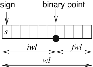
Parameters of a fixed-point number system
For fixed-point numbers, the position of the binary point is maintained after multiplications (some low-order bits are truncated or rounded). For fixed-point processors, this operation is supported by hardware.
-
Real-time capability: Some of the features of modern processors used in PCs are designed to improve the average execution time of programs. In many cases, it is difficult if not impossible to formally verify that they improve the worst case execution time. In such cases, it may be better not to implement these features. For example, it is difficult (though not impossible [4]) to guarantee a certain speed-up resulting from the use of caches. Therefore, caches are sometimes not used for embedded applications. Also, virtual addressing and demand pagingFootnote 14 are frequently not found in embedded systems. Techniques for computing worst case execution times will be presented in subsection 5.2.2.

Due to the importance of signal processing, instructions for DSP have been added to many instruction sets.
3.3.2.4 Multimedia and Short Vector Instruction Sets
Registers and arithmetic units of many modern architectures are at least 64 bit wide. Two 32 bit data types, four 16 bit data types, or eight 8 bit data types (“bytes”) can be packed into a single 64 bit register (see Fig. 3.24).

Using 64 bit registers for 16 bit data types
Arithmetic units can be designed such that they suppress carry bits at 32 bit, 16 bit, or byte boundaries. Multimedia instruction sets exploit this fact by supporting operations on packed data types. Such instructions are sometimes called single-instruction, multiple-data (SIMD) instructions, since a single instruction encodes operations on several data elements. With bytes packed into 64 bit registers, speed-ups of up to about eight over non-packed data types are possible. Data types are typically stored in packed form in memory. Unpacking and packing are avoided if arithmetic operations on packed data types are used. Furthermore, multimedia instructions can usually be combined with saturating arithmetic and therefore provide a more efficient form of overflow handling than standard instructions. Hence, the overall speed-up achieved with multimedia instructions can be significantly larger than the factor of eight enabled by operations on packed 64 bit data types. Due to the advantages of operations on packed data types, new instructions have been added to several processors. For example, so-called streaming SIMD extensions (SSE) have been added to Intel’s family of Pentium®-compatible processors [247]. New instructions have also been called short vector instructions and introduced by Intel® as Advanced Vector Extensions (AVX) [248].
3.3.2.5 Very Long Instruction Word (VLIW) Processors
Computational demands for embedded systems are increasing, especially when multimedia applications, advanced coding techniques, or cryptography are involved. Performance improvement techniques used in high-performance microprocessors are not appropriate for embedded systems: driven by the need for instruction set compatibility, processors found, for example, in PCs spend a huge amount of resources and energy on automatically finding parallelism in application programs. Still, their performance is frequently not sufficient. For embedded systems, we can exploit the fact that instruction set compatibility with PCs is not required. Therefore, we can use instructions which explicitly identify operations to be performed in parallel. This is possible with explicit parallelism instruction set computers (EPICs). With EPICs, detection of parallelism is moved from the processor to the compiler. This avoids spending silicon and energy on the detection of parallelism at run-time. As a special case, we consider very long instruction word (VLIW) processors. For VLIW processors, several operations or instructions are encoded in a long instruction word (sometimes called instruction packet) and are assumed to be executed in parallel. Each operation/instruction is encoded in a separate field of the instruction packet. Each field controls certain hardware units. Four such fields are used in Fig. 3.25, each one controlling one of the hardware units.

VLIW architecture (example)
For VLIW architectures, the compiler has to generate instruction packets. This requires that the compiler is aware of the available hardware units and schedules their use.
Instruction fields must be present, regardless of whether or not the corresponding functional unit is actually used in a certain instruction cycle. As a result, the code density of VLIW architectures may be low if insufficient parallelism is detected to keep all functional units busy. The problem can be avoided if more flexibility is added.
For example, the Texas Instruments TMS 320C6xx family of processors implements a variable instruction packet size of up to 256 bits. In each instruction field, 1 bit is reserved to indicate whether or not the operation encoded in the next field is still assumed to be executed in parallel. No instruction bits are wasted for unused functional units. Due to its variable length instruction packets, TMS 320C6xx processors do not quite correspond to the classical model of VLIW processors. Due to their explicit description of parallelism, they are EPIC processors, though.
Implementing register files for VLIW and EPIC processors is far from trivial. Due to the large number of operations that can be performed in parallel, a large number of register accesses has to be provided in parallel. Therefore, a large number of ports is required. However, the delay, size, and energy consumption of register files increase with their number of ports. Hence, register files with very large numbers of ports are inefficient. As a consequence, many VLIW/EPIC architectures use partitioned register files. Functional units are then only connected to a subset of the registers.
VLIW Pipelines
A potential problem of VLIW and EPIC architectures is their possibly large delay penalty: this delay penalty might originate from branch instructions found in some instruction packets. Instruction packets normally must pass through pipelines. Each stage of these pipelines implements only part of the operations to be performed by the instructions executed. Branch instructions cannot be detected in the first stage of the pipeline. When the execution of the branch instruction is finally completed, additional instructions have already entered the pipeline (see Fig. 3.26).

Branch instruction and delay slots
There are essentially two ways to deal with these additional instructions:
-
1.
They are executed as if no branch had been present. This case is called delayed branch. Instruction packet slots that are still executed after a branch are called branch delay slots. These branch delay slots can be filled with instructions which would be executed before the branch if there were no delay slots. However, it is normally difficult to fill all delay slots with useful instructions, and some must be filled with no-operation instructions (NOPs). The term branch delay penalty denotes the loss of performance resulting from these NOPs.
-
2.
The pipeline is stalled until instructions from the branch target address have been fetched. There are no branch delay slots in this case. In this organization, the branch delay penalty is caused by the stall.
Branch delay penalties can be significant, and efficiency can be improved by avoiding branches if possible. In order to avoid branches originating from if statements, predicated instructions have been introduced (see p. 23).
The Crusoe™ processor is a (commercially finally unsuccessful) example of an EPIC processor designed for PCs [295]. Its instruction set includes 64 bit and 128 bit VLIW instructions. Efforts for making EPIC instruction sets available in the PC sector resulted in Intel’s IA-64 instruction set [249] and its implementation in the Itanium® processor. Due to legacy problems, it has been used mainly in the server market. Many MPSoCs (see p. 36) are based on VLIW and EPIC processors.
3.3.2.6 Multi-core Processors
Processor features for single processors described above have helped to design high-performance processors in a resource-aware manner. However, it turned out that a further performance increase for single processors hits the power wall: a further increase in clock speeds would result in a too large power consumption and in too hot circuits. Further increase in the level of VLIW parallelism was not feasible either. Due to advances in fabrication technology, it is now feasible to manufacture multiple processors on the same semiconductor die. Multiple processors integrated on the same chip are called multicores. This is in contrast to multiprocessor systems which have been used in computing centers for decades. The integration of multiple cores on the same die enables a much faster communication, compared to multiprocessor systems. Also, this approach facilitates the sharing of resources (such as caches) among the cores. As an example, Fig. 3.27 demonstrates the architecture of the Intel® Core™ Duo [540].

Intel® Core™ Duo Processor
In this case, L1 caches are private, whereas L2 caches are shared. Implementing efficient accesses to caches needs some consideration [540]. With such architectures, cache coherence is becoming an issue also within one die. This means, we have to know whether updates of data and possibly also instructions by one core are seen by the others. Protocols for automatic cache coherence (like the MESI protocol) are known for many years in computer architecture [211]. Now, they have to be implemented on the chip. Scalability is an issue: for how many cores can we reasonably provide enough bandwidth in the communication architecture to always keep caches coherent? Also, the system memory bandwidth may be insufficient for a growing number of cores. Architectures other than the above Intel architecture exist.
In the architecture of Fig. 3.27, all processors are of the same type. Such an architecture is called a homogeneous multi-core architecture. Advantages of homogeneous multi-core architectures include the fact that the design effort is limited (processors will be replicated) and that software can easily be migrated from one processor to another one. This is very useful in case one of the cores fails.
In contrast to homogeneous multi-core architectures, there are also heterogeneous multi-core architectures incorporating processors of different types. Processors which are best suited for certain applications can be selected. Typically, heterogeneous architectures achieve the best energy efficiency that is feasible.
In order to find a good compromise between homogeneous and (totally) heterogeneous architectures, architectures with a single instruction set but different internal architectures, so-called single-ISA heterogeneous multi-cores [316], have been proposed. The ARM® big.LITTLE architecture is a very prominent example of this.
Figure 3.28 contains the pipeline architecture of the Cortex® -A15 processor [165].

ARM® Cortex® -A15 pipeline
It is a complex pipeline, containing multiple pipeline stages for instruction fetch, instruction decoding, instruction issue, execution, and write-back. Instructions have to pass through at least 15 pipeline stages before their result is stored. Dynamic scheduling of instructions allows executing instructions in a sequence different from the one in which they are fetched from memory (so-called out-of-order execution). Several instructions can be issued in one clock cycle (so-called multi-issue). The architecture offers a high performance but requires much power.
In contrast, Fig. 3.29 shows the pipeline of the Cortex® -A7 architecture [165].

ARM® Cortex® -A7 pipeline
It is a simple pipeline. Instructions pass through 8 to 11 stages; they are always processed in the order in which they are fetched from memory (so-called in-order execution). There are few situations in which two instructions are issued concurrently. Hence, the architecture is power-efficient but has a limited performance.
Figure 3.30 [165] demonstrates trade-offs between power consumption and performance. For each of the two architectures shown, there is flexibility for these two objectives, depending upon the supply voltage and the clock frequency.

DVFS curves for a large, representative workload on a single A7 or A15
Obviously, the Cortex® -A15 is more appropriate for more demanding high-performance applications, e.g., in video processing. The Cortex® -A7 is more appropriate for “always-on applications” like low-volume message processing. It would be a waste of energy if mobile phones would only contain Cortex® -A15 cores.
Therefore, today’s multi-core chips typically are heterogeneous in that they contain a mixture of high-performance and energy-efficient processors, as in Fig. 3.31.

ARM® big. LITTLE architecture comprising Cortex® -A7 and Cortex® -A15 cores
3.3.2.7 Graphics Processing Units (GPUs)
In the last century, many computers used specialized graphics processing units (GPUs) in order to generate an appealing graphical representation of computer output. This hardwired solution suffered from being unable to support non-standard computer graphics algorithms. Therefore, these highly specialized GPUs have been replaced by programmable solutions. Current GPUs try to run a large number of computations concurrently in order to achieve the desired performance. The standard approach to concurrency is to run many fine-grained threads at the same time. The goal is to keep many processing units busy and to hide memory latencies by fast switching between threads.
Example 3.6
Let us consider the multiplication of two large matrices on a GPU. Figure 3.32 [211] shows how the computations can be mapped to a GPU.

Partitioning of matrix multiplication for execution of a GPU
The matrix is partitioned into so-called thread blocks. Each thread block can be allocated to one of the cores contained in a GPU. Each thread block, in turn, contains a number of threads, and each thread includes a number of instructions. In Fig. 3.32, the overall set of computations is called a grid. ∇
Each core will try to achieve progress by executing threads. If some thread gets blocked, e.g., due to waiting for memory, the core will execute some other thread. The instructions contained in a thread can also be executed concurrently, e.g., by using multiple pipelines. The thread blocks can be executed concurrently on contemporary GPUs. Fast switching between the execution of threads and in this way hiding memory latencies is an essential feature for GPUs.
Example 3.7
Figure 3.33 shows the architecture of the ARM® Mali™ -T880 GPU [23].

ARM® Mali™ -T880 GPU
The architecture is defined as intellectual property (IP), comprising a synthesizable model. In this model, the number of SC cores is configurable between 1 and 16. Each core includes several pipelines for the execution of arithmetic, load/store, or texture-related instructions. In the thread issue hardware, as many threads as possible are issued each clock phase. The GPU also contains additional components like a memory management unit (see Appendix C), up to two caches and an AMBA® bus interface. Programming support includes an interface to the OpenGL library [484] and to OpenCL (see https://www.khronos.org/opencl/). ∇
In general, GPU computing achieves high performances in an energy-efficient way (see also Sect. 3.7.3 on p. 67).
3.3.2.8 Multiprocessor Systems on a Chip (MPSoCs)
Going one step further, heterogeneous multi-core systems have also been merged with GPUs.
Example 3.8
Figure 3.34 shows a contemporary heterogeneous multi-core system, also comprising a Mali GPU [22].

ARM® big.LITTLE system on a chip (SoC)
The architecture shown in Fig. 3.34 does not only contain processor cores. Rather, it comprises a number of additional system components, such as memory management units (see Appendix C) and interfaces for peripheral devices. Overall, the idea behind this integration is to avoid extra chips for such functionality. As a result, a whole system is integrated on one chip. Therefore, we are calling such an architecture a system-on-a-chip (SoC) or even a multiprocessor system-on-a-chip (MPSoC) architecture. ∇
Mapping techniques for such processors are important, since examples demonstrate that a power efficiency close to that of ASICs can be achieved. For example, for IMEC’s ADRES processor, an efficiency of 55 ∗ 109 operations per watt (about 50% of the power efficiency of ASICs) has been predicted [363, 481]. However, the design effort for such architectures is larger than in the homogeneous case.
Example 3.9
There are MPSoCs comprising processors which we introduced earlier: 66AK2x MPSoCs from Texas Instruments contain ARM® and C66xxx processors [530] (see Fig. 3.35), demonstrating relevance of the presented processors. ∇

MPSoC 66AK from Texas Instruments® containing ARM® and C6xxx processors
The number and the diversity of components can be even larger. For example, there may be specialized processors for mobile communication or image processing.
Example 3.10
Figure 3.36 contains a simplified floor-plan of the SH-MobileG1 chip [205]. The chip demonstrates that highly specialized processors are being used. There are special processors for image processing (red), for GSM and 3G mobile communication (green), etc. In order to save energy, power is shut down for unused areas, causing these areas to be a special case of dark silicon (c.f. p. 14). ∇

Floor-plan of the SH-MobileG1 chip
Specialized processors are used since progress in semiconductor manufacturing and the design of new architectures is slowing down. Hence, specialized processors are needed to meet performance targets. This view is supported by the architecture which we will present next.
Example 3.11
Around 2013, Google predicted that it would soon become very expensive to provide the expected pattern recognition performance in their data centers with conventional CPUs or GPUs. As a result, the design of specialized machine learning processors for fast classification with deep neural networks (DNNs) was started with a high priority. The resulting so-called Tensor Processing Unit (TPU) architecture is shown in Fig. 3.37.

At the core of the architecture, there is a 256 by 256 array of MAC units. 64k 8 bit MAC operations can be performed in a single cycle; 16 bit operations require more cycles. DNNs consist of layers of computations, where at each layer MAC operations involving weight factors are required. These are performed by “pumping” input data or data from intermediate layers through the MAC matrix. Each cycle, 256 result values become available. TPU version 1 outperforms commonly used CPUs and GPUs by a factor of 29.2 and 13.3, respectively. The performance/power ratio is improved by factors of 34 and 16, respectively. More recently, Google announced second- and third-generation TPUs [93]. They do also support training DNNs. ∇
3.3.3 Reconfigurable Logic
In many cases, full-custom hardware chips (ASICs) are too expensive, and software-based solutions are too slow or too energy-consuming. Reconfigurable logic provides a solution if algorithms can be efficiently implemented in custom hardware. It can be almost as fast as special-purpose hardware, but in contrast to special-purpose hardware, the performed function can be changed by using configuration data. Due to these properties, reconfigurable logic finds applications in the following areas:
-
Fast prototyping: Modern ASICs can be very complex and the design effort can be large and take a long time. It is therefore frequently desirable to generate a prototype, which can be used for experimenting with a system which behaves “almost” like the final system. The prototype can be more costly and larger than the final system. Also, its power consumption can be larger than the final system, some timing constraints can be relaxed, and only the essential functions need to be available. Such a system can then be used for checking the fundamental behavior of the future system.
-
Low-volume applications: If the expected market volume is too small to justify the development of special-purpose ASICs, reconfigurable logic can be the right hardware technology for applications, for which software would be too slow or too inefficient.
-
Real-time systems: The timing of reconfigurable logic-based designs is typically known very precisely. Therefore, they can be used to implement timing-predictable systems.
-
Applications benefiting from a very high level of parallel processing: For example, parallel searches for certain patterns can be implemented as parallel hardware. Therefore, reconfigurable logic is employed in searches for genetic information, for patterns in Internet messages, in stock data, in seismic analysis, and more.
Reconfigurable hardware frequently includes random access memory (RAM) to store configurations. We distinguish between persistent and volatile configuration memory. For persistent memory, information is retained when power is shut off. For volatile memory, the information is lost once power is shut down. If the configuration memory is volatile, its content must be loaded from some persistent storage technology such as read-only memories (ROMs) or flash memories at startup.
Field programmable gate arrays (FPGAs) are the most common form of reconfigurable hardware. As the name indicates, such devices are programmable “in the field” (after fabrication). Furthermore, they consist of arrays of processing elements. As an example, Fig. 3.38 shows the column-based structure of the Xilinx® UltraScale architecture [602].Footnote 15 Some columns contain I/O interfaces, clock devices, and/or RAM. Other columns comprise configurable logic blocks (CLBs), special hardware for digital signal processing, and some RAM. CLBs are the key components. They provide configurable functions. The architecture of Xilinx® UltraScale CLBs is shown in Fig. 3.39 [599].

Floor-plan of column-based Xilinx® UltraScale FPGAs

Xilinx® UltraScale CLB (one of eight blocks shown)
In this architecture, each CLB contains eight blocks. Each block comprises a RAM which is used to implement logic functions by a look-up table (LUT, shown in red), two registers, multiplexers, and some additional logic. Each LUT has six address inputs and two outputs. It can implement any single Boolean function of six variables or two functions of five variables (provided that the two functions share input variables). This means that all 264 functions of 6 variables or all 232 functions of 5 inputs can be implemented! This is the key means for achieving configurability. In addition, the logic contained in such a block can also be configured. This includes the control of the two registers, which can be programmed to store results of the LUT or some direct input values. Blocks in a CLB can be combined to form adders, multiplexers, shift registers, or memories. Configuration data determines the setting of multiplexers in the CLBs, the clocking of registers and RAM, the content of RAM components, and the connections between CLBs. Some of the LUTs can also be used as RAM. A single CLB can store up to 512 bits.
Several CLBs can be combined to create, for example, adders having a larger bit width, memories having a larger capacity, or complex logic functions.
Currently available FPGAs comprise a large number of specialized blocks, like hardware for digital signal processing (DSP), some memory, high-speed I/O devices for various I/O standards, a decryption facility for FPGA configuration data, debugging support, ADCs, high-speed clocking, etc.
Example 3.12
Virtex® UltraScale™ VU13P devices include 1728 k LUTs, 48 Mbit distributed RAM, 94.5 Mbit “Block RAM,” 360 Mbit “UltraRAM,” about 12 k specialized DSP devices, 4 PCIe® devices, Ethernet interfaces, and up to 832 I/O pins [601]. ∇
Integration of reconfigurable computing with processors and software is simplified if processors are available in the FPGAs. There may be either hard cores or soft cores. For hard cores, the layout contains a special area implementing a core in a dense way. This area cannot be used for anything but the hard core. Soft cores are available as synthesizable models which are mapped to standard CLBs. Soft cores are more flexible but less efficient than hard cores. Soft cores can be implemented on any FPGA chip.
Example 3.13
The MicroBlaze processor [598] is an example of a soft core. ∇
Example 3.14
At the time of writing this book, hard cores are available, for example, on Zynq UltraScale+ MPSoCs. They contain up to four ARM® Cortex-A53 cores, two ARM Cortex-R5 cores, and a Mali-400MP2 GPU processor [602]. ∇
Typically, configuration data is generated from a high-level description of the functionality of the hardware, for example, in VHDL. FPGA vendors provide the necessary design kits. Ideally, the same description could also be used for generating ASICs automatically. In practice, some interaction is required. Exploitation of the available parallelism typically requires manually parallelized applications, since automatic parallelization is frequently very limited. The parallelism offered by FPGAs is typically not fully exploited if all computations are mapped to processor cores. Overall, FPGAs allow implementing a huge variety of hardware devices without any need to create hardware other than FPGA boards.
Example 3.15
Currently (in 2020), alternate providers of FPGAs include Altera® (see http://www.altera.com, acquired by Intel®), Lattice Semiconductor (see http://www.latticesemi.com), QuickLogic (see http://www.quicklogic.com), Microsemi (formerly Actel; see http://www.microsemi.com), and Chinese vendors. ∇
3.4 Memories
3.4.1 Conflicting Goals
Data, programs, and FPGA configurations must be stored in some kind of memory. Memories must have a capacity as large as required by the applications, provide the expected performance, and still be efficient in terms of cost, size, and energy consumption. Requirements for memories also include the expected reliability and access granularity (e.g., bytes, words, pages). Furthermore, we distinguish between persistent and volatile memory (see p. 39). The mentioned requirements are conflicting, as has already been observed by Burks, Goldstine, and von Neumann in 1946 [78]:
“Ideally one would desire an indefinitely large memory capacity such that any particular …word …would be immediately available — i.e. in a time which is …shorter than the operation time of a fast electronic multiplier. …It does not seem possible physically to achieve such a capacity.”
Access times of some currently available memories can be estimated with CACTI. These estimates are based on the tentative generation of a memory layout and the extraction of capacitances [589]. Many different parameters enable the selection of an appropriate fabrication technology.Footnote 16
Example 3.16
Figure 3.40 shows the results for a range of exponentially increasing sizes [36]. Obviously, the access time increases as a function of the capacity of memories: the larger the memory, the longer it takes to access information. In addition, Fig. 3.40 also includes the energy consumption. Large memories also tend to be energy-inefficient. The impact of the capacity of the memory on the energy consumption is even larger than the impact on the access time. ∇

Delay and access time of random access memory as predicted by CACTI
For a number of years, the difference in speeds between processors and memories increased (see Fig. 3.41) until processor clock rates saturated (around 2003). While the speed of memories increased by only a factor of about 1.07 per year, overall processor performance increased by a factor of 1.5–2 per year [358]. Overall, the gap between processor performance and memory speeds has become large. Accordingly, a further increase of the overall performance is made at least very difficult due to memory access times. This fact has also been called the memory wall [358]. Further increase of clock rates of single processors has come to a standstill, but the large gap remains which existed when clock speeds became essentially saturated and multi-cores require additional memory bandwidth. As a result, we have to find compromises between the different requirements for the memory architecture.

Historical speed gap increase (until about 2003)
3.4.2 Memory Hierarchies
Due to the observed conflicts, Burks, Goldstine, and von Neumann wrote already in 1946 [78]: “We are therefore forced to recognize the possibility of constructing a hierarchy of memories, each of which has greater capacity than the preceding but which is less quickly accessible.”
The exact structure of the hierarchy depends on technological parameters and also on the application area. Typically, we can identify at least the following levels in the memory hierarchy:
-
Processor registers can be seen as the fastest level in the memory hierarchy, with only a limited capacity of at most a few hundred words.
-
The working memory (or main memory) of computer systems implements the storage implied by processor memory addresses. Usually it has a capacity between a few megabytes and some gigabytes and is volatile.
-
Typically there is a large access speed difference between the main memory and registers. Hence, many systems include some type of buffer memory. Frequently used buffer memories include caches, translation look-aside buffers (TLBs; see Appendix C), and scratchpad memory (SPM). In contrast to PC-like systems and compute servers, the architecture of these small memories should guarantee a predictable real-time performance. A combination of small memories containing frequently used data and instructions and a larger memory containing the remaining data and instructions is generally also more energy efficient than a single, large memory.
-
Memories introduced so far are normally implemented in volatile memory technologies. In order to provide persistent storage, some different memory technology must be used. For embedded systems, flash memory is frequently the best solution. In other cases, hard disks or Internet-based storage solutions (like the “cloud”) may be used.
Memory hierarchies can be exploited in order to achieve a compromise between the design goals for the memory. Memory partitioning has been considered, for example, by A. Macii [360]. New memory technologies (including persistent memories) have the potential to change currently dominating hierarchies [388].
3.4.3 Register Files
The mentioned impact of the storage capacity on access times and energy consumption applies even to small memories such as register files. Figure 3.42 shows the cycle time and the power as a function of the size of memories used as register files [471]. The power needs to be considered due to frequent accesses to registers, as a result of which they can get very hot.

Cycle time and power as a function of the register file size
3.4.4 Caches
For caches it is required that the hardware checks whether or not the cache has a valid copy of the information associated with a certain address. This check involves comparing the tag fields of caches, containing a subset of the relevant address bits [211]. If the cache has no valid copy, the information in the cache is automatically updated.
Caches were initially introduced in order to provide good run-time efficiency. The name is derived from the French word cacher (to hide), indicating that programmers do not need to see or to be aware of caches, since updating information in caches is automatic. However, when large amounts of information need to be accessed, caches are not so invisible anymore. This has been demonstrated very nicely by Drepper [139]. Drepper analyzed execution times of a program traversing a linear list of entries. Each entry contained one 64 bit pointer to the next entry plus NPAD 64 bit words. Execution times were measured for a Pentium P4 processor comprising a 16 kB level 1 cache requiring 4 processor cycles per access, a 1 MB level 2 cache requiring 14 processor cycles per access, and a main memory requiring 200 cycles per access. Figure 3.43 shows the average number of cycles per access to one list element as a function of the total size of the list for the case NPAD=0. For small sizes of the list, four cycles are required per list element. This means that we are almost always accessing the level 1 cache, since it is large enough for this size of the list. If we increase the size of the list, we need eight cycles per access on average. In this case, we are accessing the level 2 cache. However, since the cache block size is large enough to hold two list elements, only every second access is actually an access to the level 2 cache. For even larger lists, the access time increases to nine cycles. In these cases, the list is larger than the level 2 cache, but automatic prefetching of level 2 cache entries hides some of the access latency of the main memory.

Average number of cycles per access for NPAD=0
Figure 3.44 shows the average number of cycles per access to one list element as a function of the total size of the list for cases NPAD=0, 7, 15, and 31. For NPAD=7, 15, and 31, prefetching fails due to the larger size of list items. Obviously, we see a dramatic increase of access times. This means that the cache architecture has a strong impact on the execution times of applications. Increasing cache size will only change the size of the application at which this increase in execution times happens. Clever exploitation of hierarchies can have a large impact on execution times.

Average number of cycles per access for NPAD=0, 7, 15, 31
So far, we have just looked at the impact of capacity on access times. In the context of Fig. 3.40 however, it is obvious that caches potentially also improve the energy efficiency of a memory system. Accesses to caches are accesses to small memories and therefore require less energy per access than large memories.
Predicting cache misses and hits at design time is difficult and is a burden for the accurate prediction of real-time performance (see p. 246).
3.4.5 Scratchpad Memories
Alternatively, small memories can be mapped into the address space (see Fig. 3.45).

Memory map with scratchpad included
Such memories are called scratchpad memories (SPMs) or tightly coupled memories (TCM). SPMs are accessed by a proper selection of memory addresses. There is no need for checking tags, as for caches. Instead, the SPM is accessed whenever some simple address decoder is signaling an address to be in the address range of the SPM. SPMs are typically integrated together with processors on the same die. Hence, they are a special case of on-chip memories. For n-way set associative caches, reads are usually reading n entries in parallel and select the right entry only afterward. These energy-hungry parallel reads are avoided for SPMs. As a result, SPMs are very energy-efficient.
Figure 3.46 shows a comparison between the energy required per access to the scratchpad (SPM) and the energy required per access to the cache.

Energy consumption per scratchpad and cache access
For a two-way set associative cache, the two values differ by a factor of about three. The values in this example were computed using the energy consumption for RAM arrays as estimated by CACTI [589]. A detailed comparison between figures of merit for caches and scratchpads was published by Banakar et al. [36].
Frequently used variables and instructions should be allocated to the address space of SPMs. SPMs can improve the memory access times very predictably if the compiler is in charge of keeping frequently used variables in the SPM (see p. 363).
3.5 Communication
Information must be communicated before it can be processed in an embedded system. Communication is particularly important for the Internet of Things. Information can be communicated through various channels. Channels are abstract entities characterized by the essential properties of communication, like maximum information transfer capacity and noise parameters. The probability of communication errors can be computed using communication theory techniques. The physical entities enabling communication are called communication media. Important media classes include wireless media (radio frequency media, infrared), optical media (fibers), and wires.
There is a huge variety of communication requirements between the various classes of embedded systems. In general, connecting the different embedded hardware components is far from trivial. Some common requirements can be identified.
3.5.1 Requirements
The following list contains some of the requirements that must be met:
-
Real-time behavior: This requirement has far-reaching consequences on the design of the communication system. Several low-cost solutions such as standard Ethernet fail to meet this requirement.
-
Efficiency: Connecting different hardware components can be expensive. For example, point-to-point connections in large buildings are almost impossible. Also, it has been found that separate wires between control units and external devices in cars significantly add to the cost and the weight of the car. With separate wires, it is also difficult to add new components. The need for cost efficiency also affects the way in which power is made available to external devices. There is frequently the need to use a central power supply to reduce the cost.
-
Appropriate bandwidth and communication delay: Bandwidth requirements of embedded systems may vary. It is important to provide sufficient bandwidth without making the communication system too expensive.
-
Support for event-driven communication: Polling-based systems provide a very predictable real-time behavior. However, their communication delay may be too large, and there should be mechanisms for fast, event-oriented communication. For example, emergency situations should be communicated immediately and should not remain unnoticed until some central controller polls for messages.
-
Security/privacy: Ensuring security/privacy of confidential information (confidentiality) may require the use of encryption.
-
Safety/robustness: For safety-critical systems, the required level of safety must be achieved. This includes robustness: cyber-physical systems may be used at extreme temperatures, close to major sources of electromagnetic radiation, etc. Car engines, for example, can be exposed to temperatures of, e.g., less than − 20 and up to + 180∘C (− 4–356 ∘F). Voltage levels and clock frequencies could be affected due to this large variation in temperatures. Still, reliable communication must be maintained.
-
Fault tolerance: Despite all the efforts for robustness, faults may occur. Cyber-physical systems should be operational even after faults, if at all feasible. Restarts, like the ones found in PCs, cannot be accepted. This means that retries may be required after attempts to communicate failed. A conflict exists with the first requirement: if we allow retries, then it is difficult to meet real-time requirements.
-
Maintainability, diagnosability: Obviously, it should be possible to repair embedded systems within reasonable time frames.
These communication requirements are a direct consequence of the general characteristics of embedded/cyber-physical systems mentioned in Chap. 1. Due to the conflicts between some of the requirements, compromises must be made. For example, there may be different communication modes: one high-bandwidth mode guaranteeing real-time behavior but no fault tolerance (this mode is appropriate for multimedia streams) and a second fault-tolerant, low-bandwidth mode for short messages that must not be dropped.
3.5.2 Electrical Robustness
There are some basic techniques for electrical robustness. Digital communication within chips is normally using so-called single-ended signaling. For single-ended signaling, signals are propagated on a single wire (see Fig. 3.47).

Single-ended signaling
Such signals are represented by voltages with respect to a common ground (less frequently by currents). A single ground wire is sufficient for a number of single-ended signals. Single-ended signaling is very much susceptible to external noise. If external noise (originating from, e.g., motors being switched on) affects the voltage, messages can easily be corrupted. Also, it is difficult to establish high-quality common ground signals between a large number of communicating systems, due to the resistance (and self-inductance) on the ground wires. This is different for differential signaling. For differential signaling, each signal needs two wires (see Fig. 3.48).

Differential signaling
Using differential signaling, binary values are encoded as follows: if the voltage on the first wire with respect to the second is positive, then this is decoded as ’1’; otherwise values are decoded as ’0’. The two wires will typically be twisted to form so-called twisted pairs. There will be local ground signals, but a non-zero voltage between the local ground signals does not hurt. Advantages of differential signaling include the following:
-
Noise is added to the two wires in essentially the same way. The comparator therefore removes almost all the noise.
-
The logic value depends just on the polarity of the voltage between the two wires. The magnitude of the voltage can be affected by reflections or because of the resistance of the wires; this has no effect on the decoded value.
-
Signals do not generate any currents on the ground wires. Hence, the quality of the ground wires becomes less important.
-
No common ground wire is required. Hence, there is no need to establish a high-quality ground wiring between a large number of communicating partners.
-
As a consequence of the properties mentioned so far, differential signaling allows a larger throughput than single-ended signaling.
However, differential signaling requires two wires for every signal, and it also requires negative voltages (unless it is based on complementary logic signals using voltages for single-ended signals). Differential signaling is used, for example, in standard Ethernet-based networks and the universal serial bus (USB).
3.5.3 Guaranteeing Real-Time Behavior
For internal communication, computers may be using dedicated point-to-point communication or shared buses. Point-to-point communication can have a good real-time behavior but requires many connections, and there may be congestion at the receivers. Wiring is easier with common, shared buses. Typically, such buses use priority-based arbitration if several access requests to the communication media exist (see, e.g., [211]). Priority-based arbitration comes with poor timing predictability, since conflicts are difficult to anticipate at design time. Priority-based schemes can even lead to “starvation” (low-priority communication can be completely blocked by higher-priority communication). In order to get around this problem, time division multiple access (TDMA) can be used. In a TDMA scheme, each partner is assigned a fixed time slot. The partner is only allowed to transmit during that particular time slot. Typically, communication time is divided into frames. Each frame starts with some time slot for frame synchronization and possibly some gap to allow the sender to turn off (see Fig. 3.49, [302]).

TDMA-based communication
This gap is followed by a number of slices, each of which serves for communicating messages. Each slice also contains some gap and guard time to take clock speed variations of the partners into account. Slices are assigned to communication partners. Variations of this scheme exist. For example, truncation of unused slices or the assignment of partners to several slices are feasible. TDMA reduces the maximum amount of data available per frame and partner but guarantees a certain bandwidth for all partners. Starvation can be avoided. The ARM AMBA bus [21] includes TDMA-based bus allocation.
Communication between computers is frequently based on Ethernet standards. For 10 and 100 Mbit/s versions of Ethernet, there can be collisions between various communication partners. This means several partners are trying to communicate at about the same time and the signals on the wires are corrupted. Whenever this occurs, the partners must stop communications, wait for some time, and then retry. The waiting time is chosen at random, so that it is not very likely that the next attempt to communicate results in another collision. This method is called carrier-sense multiple access with collision detection (CSMA/CD). For CSMA/CD, communication time can become huge, since conflicts can repeat a large number of times, even though this is not very likely. Hence, CSMA/CD cannot be used when real-time constraints must be met.
This problem can be solved with CSMA/CA (carrier-sense multiple access with collision avoidance). As the name indicates, collisions are completely avoided, rather than just detected. For CSMA/CA, priorities are assigned to all partners. Communication media are allocated to communication partners during arbitration phases, which follow communication phases. During arbitration phases, partners wanting to communicate indicate this on the media. Partners finding such indications of higher priority must immediately remove their indication.
Provided that there is an upper bound on the time between arbitration phases, CSMA/CA guarantees a predictable real-time behavior for the partner having the highest priority. For other partners, real-time behavior can be guaranteed if the higher priority partners do not continuously request access to the media.
Note that high-speed versions of Ethernet (≥1 Gbit/s) also avoid collisions. TDMA schemes are also used for wireless communication. For example, mobile phone standards like GSM use TDMA for accesses to the communication medium.
3.5.4 Examples
-
Sensor/actuator buses: Sensor/actuator buses provide communication between simple devices such as switches or lamps and the processing equipment. There may be many such devices and the cost of the wiring needs special attention for such buses.
-
Field buses: Field buses are similar to sensor/actuator buses. In general, they are supposed to support larger data rates than sensor/actuator buses. Examples of field buses include the following:
-
Controller Area Network (CAN): This bus was developed in 1981 by Bosch and Intel for connecting controllers and peripherals. It is popular in the automotive industry, since it allows the replacement of a large amount of wires by a single bus. Due to the size of the automotive market, CAN components are relatively cheap and are therefore also used in other areas such as smart homes and fabrication equipment. CAN is based on differential signaling and arbitration using CSMA/CA. The encoding of signals is similar to that of serial (RS-232) lines of early PCs, with modifications for differential signaling. CSMA/CA-based arbitration does not prevent starvation. This is an inherent problem of the CAN protocol. Extensions exist.
-
The Time-Triggered Protocol (TTP) [304]: This is a protocol for fault-tolerant safety systems like airbags in cars.
-
FlexRay ™ [253] : This is a TDMA protocol which has been developed by the FlexRay consortium (BMW, Daimler AG, General Motors, Ford, Bosch, Motorola, and Philips Semiconductors).
FlexRay includes a static as well as a dynamic arbitration phase. The static phase uses a TDMA-like arbitration scheme. It can be used for real-time communication and starvation can be avoided. The dynamic phase provides a good bandwidth for non-real-time communication. Communicating partners can be connected to up to two buses for fault-tolerance reasons. Bus guardians may protect partners against partners flooding the bus with redundant messages, so-called babbling idiots. Partners may use their own local clock periods. Periods common to all partners are defined as multiples of such local clock periods. Time slots allocated to partners for communication are based on these common periods.
The levi simulation allows simulating the protocol in a lab environment [495].
-
LIN (Local Interconnect Network): This is a low-cost communication standard for connecting sensors and actuators in the automotive domain [346].
-
MAP: MAP is a bus designed for car factories.
-
EIB: The European Installation Bus (EIB) is a bus designed for smart homes.
-
-
The Inter-Integrated Circuit (I2C) Bus : This is a simple low-cost bus designed to communicate at short distances (meter range) with relatively low data rates. The bus needs only four wires: ground, SCL (clock), SDA (data), and a voltage supply line. Data and clock lines are open collector lines (see pp. 61–63). This means that connected devices pull these lines only toward ground. Separate resistors are needed to pull these lines up. The standard speed of I2C is 100 kb/s, but versions for 10 kb/s and up to 3.4 Mb/s do also exist. The voltage on the supply voltage line may vary between interfaces. Only the standards for detecting high and low logic levels are defined relative to the supply voltage. The bus is supported on some micro-controller boards.
-
Wired multimedia communication: For wired multimedia communication, larger data rates are required. For example, MOST (Media Oriented Systems Transport) is a communication standard for multimedia and infotainment equipment in the automotive domain [402]. Standards like IEEE 1394 (FireWire) may be used for the same purpose.
-
Wireless communication: This kind of communication is becoming more popular. Standards for wireless communication include the following:
-
Mobile communication is becoming available at increased data rates. 7 Mbit/s are obtained with HSPA (High Speed Packet Access). About ten times higher rates are available with long-term evolution (LTE). 5G networks are expected to provide data rates between 50 Mbit/s and more than a gigabit/s, with latencies less than those of earlier networks.
-
Bluetooth is a standard for connecting devices such as mobile phones and their headsets over short distances.
-
Wireless local area networks (WLANs) are standardized as IEEE standard 802.11, with several supplementary standards.
-
ZigBee (see http://www.zigbee.org) is a communication protocol designed to create personal area networks using low-power radios. Applications include home automation and the Internet of Things.
-
Digital European cordless telecommunications (DECT) is a standard used for wireless phones. It is being used throughout the world, except for different frequencies used in North America (see https://en.wikipedia.org/wiki/Digital_Enhanced_Cordless_Telecommunications).
-
3.6 Output: Interface Between Cyber and Physical World
Output devices are key components of the cyphy-interface. Examples include:
-
Displays: Display technology is an area which is extremely important. Accordingly, a large amount of information [503] exists on this technology. Major research and development efforts lead to new display technology such as organic displays [342]. Organic displays are emitting light and can be fabricated with very high densities. In contrast to LCDs, they do not need backlight and polarizing filters. Major changes are therefore expected in these markets.
-
Electro-mechanical devices: These influence the environment through motors and other electro-mechanical equipment.
Analog as well as digital output devices are used. In the case of analog output devices, the digital information must first be converted by digital-to-analog converters (DACs). These converters can be found on the path from analog inputs of embedded systems to their outputs. Figure 3.50 shows the naming convention of signals along the path which we use. Purpose and function of the boxes will be explained in this section.

Naming convention for signals between analog inputs and outputs
3.6.1 Digital-to-Analog Converters
Digital-to-analog converters (DACs) are also included in the cyphy-interface. They are not very complex. Figure 3.51 shows the schematic of a simple so-called weighted-resistor DAC.

DAC
The key idea of the converter is to first generate a current which is proportional to the value represented by a digital signal x. Such a current can hardly be used by a following system. Therefore, this current is converted into a proportional voltage y. This conversion is done with an operational amplifier (depicted by a triangle in Fig. 3.51). Essential characteristics of operational amplifiers are described in Appendix B of this book.
How do we compute the output voltage y? Consider the four resistors on the left in Fig. 3.51. The current through any resistor is zero if the corresponding element of digital signal x is ’0’. If it is ’1’, the current corresponds to the weight of that bit, since resistor values are chosen accordingly. Now, consider the loop indicated by the red dashed line in Fig. 3.51. We can apply Kirchhoff’s loop rule (see Appendix B) to the loop turned on by the least significant bit x 0 of x. Let us start the loop traversal at the corresponding resistor and continue in a clockwise fashion. The second term is the voltage V − between the inputs of the operational amplifier, counted as positive, since we proceed in the direction of the arrow. The third term is contributed by the constant voltage source, counted as negative, since we proceed against the direction of the arrow. Overall, we have
V − is approximately 0 (see Appendix B, Eq. (B.14)). Therefore, we have
Corresponding equations hold for the currents I 1 to I 3 through the other resistors. We can now apply Kirchhoff’s node rule to the circuit node connecting all resistors. At this node, the outgoing current must be equal to the sum of the incoming currents. Therefore, we have
Now, we can apply Kirchhoff’s loop rule to the loop comprising R 1, y, and V −. Since V − is approximately 0, we have
Next, we can apply Kirchhoff’s node rule to the node connecting I, I′, and the inverting signal input of the operational amplifier. The current into this input is practically zero, and currents I and I′ are equal: I = I′. Hence, we have
From Eqs. (3.25) and (3.27), we obtain
nat denotes the natural number represented by digital signal x. Obviously, y is proportional to the value represented by x. Positive output voltages and bit vectors representing two’s complement numbers require minor extensions.
From a DSP point of view, y(t) is a function over a discrete time domain: it provides us with a sequence of voltage levels. In our running example, it is defined only over integer times. From a practical point of view, this is inconvenient, since we would typically observe the output of the circuit of Fig. 3.51 continuously. Therefore, DACs are frequently extended by a “zero-order hold” functionality. This means that the converter will keep the previous value until the next value is converted. Actually, the DAC of Fig. 3.51 will do exactly this if we do not change the settings of the switches until the next discrete time instant. Hence, the output of the converter is a step function y′(t) corresponding to the sequence y(t).Footnote 17 y′(t) is a function over the continuous time domain.
As an example, let us consider the output resulting from the conversion of the signal of Eq. (3.3), assuming a resolution of 0.125. For this case, Fig. 3.52 shows y′(t) instead of y(t), since y′(t) is a bit easier to visualize.

y′(t) (red) generated from signal e 3(t) (blue) (Eq. (3.3)) sampled at integer times
DACs enable a conversion from time- and value-discrete signals to signals in the continuous time and value domain. However, neither y(t) nor y′(t) reflects the values of the input signal in between the sampling instances.
3.6.2 Sampling Theorem
Suppose that the processors used in the hardware loop forward values from ADCs unchanged to the DACs. We could also think of storing values x(t) on a CD and aiming at generating an excellent analog audio signal. Would it be possible to reconstruct the original analog voltage e(t) (see Figs. 3.8, 3.21, and 3.50) at the outputs of the DACs?
It is obvious that reconstruction is not possible if we have aliasing of the type described in Fig. 3.7 on p. 8.Footnote 18 So, we assume that the sampling rate is larger than twice the highest frequency of the decomposition of the input signal into sine waves (sampling criterion; see Eq. (3.8)). Does meeting this criterion allow us to reconstruct the original signal? Let us have a closer look!
Feeding DACs with a discrete sequence of digital values will result in a sequence of analog values being generated. Values of the input signal in between the sampling instances are not generated by DACs. The simple zero-order hold functionality (if present) would generate only step functions. This seems to indicate that reconstruction of e(t) would require an infinitely large sampling rate, such that all intermediate values can be generated.
However, there could be some kind of smart interpolation computing values in between the sampling instances from the values at sampling instances. And indeed, sampling theory [440] tells us that a corresponding time-continuous signal z(t) can be constructed from the sequence y(t) of analog values.
Let {t s}, s = …, −1, 0, 1, 2, … be the time points at which we sample our input signal. Let us assume a constant sampling rate of \(f_s=\frac {1}{T_s}\) (∀s : T s = t s+1 − t s). Then, sampling theory tells us that we can approximate e(t) from y(t) as follows:
This equation is known as the Shannon-Whittaker interpolation. y(t s) is the contribution of signal y at sampling instance t s. This means, all 264 Boolean functions of 6 inputs respectively all 232 Boolean functions of 5 inputs can be implemented. The decrease follows a weighting factor, also known as the sinc function
which decreases non-monotonically as a function of |t − t s|. This weighting factor is used to compute values in between the sampling instances. Figure 3.53 shows the weighting factor for the case T s = 1.

Visualization of Eq. (3.30) used for interpolation
Using the sinc function, we can compute the terms of the sum in Eq. (3.29). Figures 3.54 and 3.55 show the resulting terms if e(t) = e 3(t) and processing performs the identify function (x(t) = w(t)).

y′(t) (red) and the first three terms of Eq. (3.29)

y′(t) (red) and the last three non-zero terms of Eq. (3.29)
At each of the sampling instances t s (integer times in our case), z(t s) is computed just from the corresponding value y(t s), since the sinc function is zero in this case for all other sampled values. In between the sampling instances, all of the adjacent discrete values contribute to the resulting value of z(t). Figure 3.56 shows the resulting z(t) if e(t) = e 3(t) and processing performs the identify function (x(t) = w(t)).

e 3(t) (blue), y′(t) (red), z(t) (magenta)
The figure includes signals e 3(t) (blue), y′(t) (red), and z(t) (magenta). z(t) is computed by summing up the contributions of all sampling instances shown in the diagrams in Figs. 3.54 and 3.55. e 3(t) and z(t) are very similar.
How close could we get to the original input signal by implementing Eq. (3.29)? Sampling theory tells us (see, e.g., [440]) that Eq. ( 3.29 ) computes an exact approximation if the sampling criterion (Eq. (3.8)) is met. Therefore, let us see how we can implement Eq. (3.29).
How do we compute Eq. (3.29) in an electronic system? We cannot compute this equation in the discrete time domain using a digital signal processor for this, since this computation has to generate a time-continuous signal. Computing such a complex equation with analog circuits seems to be difficult at first sight.
Fortunately, the required computation is a so-called folding operation between signal y(t) and the sinc function. According to the classical theory of Fourier transforms, a folding operation in the time domain is equivalent to a multiplication with frequency-dependent filter function in the frequency domain. This filter function is the Fourier transform of the corresponding function in the time domain. Therefore, Eq. (3.29) can be computed with some appropriate filter. Figure 3.57 shows the corresponding placement of the filter.

Converting signal e(t) from the analog time/value domain to the digital domain and back
Which frequency-dependent filter function is the Fourier transform of the sinc function? Computing the Fourier transform of the sinc function yields a low-pass filter function [440]. So, “all” we must do to compute Eq. (3.29) is to pass signal y(t) through a low-pass filter, filtering frequencies as shown for the ideal filter in Fig. 3.58. The representation of function y(t) as a sum of sine waves would require very high-frequency components, making such a filtering non-redundant, even though we have already assumed an anti-aliasing filter to be present at the input.

Low-pass filter: ideal (blue, dashed) and realistic (red, solid)
Unfortunately, ideal low-pass filters do not exist. We must live with compromises and design filters approximating the low-pass filters. Actually, we must live with several imperfections preventing a precise reconstruction of the input signals:
-
Ideal low-pass filters cannot be designed. Therefore, we must use approximations of such filters. Designing good compromises is an art (performed extensively, e.g., for audio equipment).
-
Similarly, we cannot completely remove input frequencies beyond the Nyquist frequency.
-
The impact of value quantization is visible in Fig. 3.56. Due to value quantization, e 3(t) is sometimes different from z(t). Quantization noise, as introduced by ADCs, cannot be removed during output generation. Signal w(t) from the output of the ADC will remain distorted by the quantization noise. However, this effect does not affect the signal h(t) from the output of sample-and-hold circuits.
-
Equation (3.29) is based on an infinite sum, involving also values at future instances in time. In practice, we can delay signals by some finite amount to know a finite number of “future” samples. Infinite delays are impossible. In Fig. 3.56, we did not consider contributions of sampling instances outside the diagram.
The functionality provided by low-pass filters demonstrates the power of analog circuits: there would be no way of implementing the behavior of analog filters in the digital domain, due to the inherent restriction to discretized time and values.
Many authors have contributed to sampling theory. Therefore, many names can be associated with the sampling theorem. Contributors include Shannon, Whittaker, Kotelnikov, Nyquist, Küpfmüller, and others. Therefore, the fact that the original signal can be reconstructed should simply be called the sampling theorem, since there is no way of attaching all names of relevant contributors to the theorem.
3.6.3 Pulse-Width Modulation
In practice, the presented generation of analog signals has a number of disadvantages:
-
DACs using an array of resistors are difficult to build. The precision of the resistors must be excellent. The deviation of the resistor handling the most significant bit from its nominal value must be less than the overall resolution of the converter. For example, this means that, for a 14 bit converter, the deviation of the real resistance from its nominal value must be in the order of 0.01%. This precision is difficult to achieve in practice, in particular over the full temperature range. If this precision is not achieved, the converter is not linear, possibly not even monotone.
-
In order to generate a sufficient power for motors, lamps, loudspeakers, etc., analog outputs would need to be amplified in a power amplifier. Analog power amplifiers, such as so-called class A power amplifiers, are very power-inefficient, since they contain an always conducting path between the two rails of the power supply. This path results in a constant power consumption, irrespective of the actual output signal. For very small output signals, the ratio between the actually used power and the consumed power is therefore very small. As a result, the efficiency of audio power amplifiers for low-volume audio would be terribly bad.
-
It is not easy to integrate analog circuitry on digital micro-controller chips. Adding external analog active components increases costs substantially.
Therefore, pulse-width modulation (PWM) is very popular. With PWM, we are using a digital output and generate a digital signal whose duty cycle corresponds to the value to be converted. Figure 3.59 shows digital signals with duty cycles of 25% and 75%. Such signals can be represented by Fourier series like in Eq. (3.1). For applications of PWM, we try to eliminate effects of higher-frequency components.

Duty cycles
PWM signals can be generated by comparing a counter against a value stored in a programmable register (see Fig. 3.60). A high voltage is output whenever the value in the counter exceeds the value in the register. Otherwise, a voltage close to zero is generated. The clock signal of the counter must be programmable to select the basic frequency of the PWM signals. In our schematic, we have assumed that the PWM frequency is identical for all PWM outputs. Registers must be loaded with the values to be converted, typically at the sampling rate of the analog signals.

Hardware for PWM output
The effort required for filtering higher-frequency components depends upon the application. For driving a motor, the averaging takes place in the motor, due to the mass of the moving parts in the motor and possibly also due to the self-inductance of the motor. Hence, no external components are needed (see Fig. 3.60). For lamps, the averaging takes place in the human eye, as long as the frequencies are not too low. It may also be okay to drive simple buzzers directly. In other cases, filtering out higher-frequency components may be needed. For example, electromagnetic radiation caused by higher-frequency components may be unacceptable, or audio applications may be demanding filtered high-frequency signals. In Fig. 3.60, two capacitors and one inductor have been used to filter out high-frequency components for the loudspeakers. In our example, we are showing four PWM outputs. Having several PWM outputs is a common situation. For example, Atmel 32 bit AVR micro-controllers in the AT32UC3A Series have seven PWM outputs [27]. In practice, there are many options for the detailed behavior of PWM hardware.
The choice of the basic frequency (the reciprocal of the period) of the PWM signal and the filter is a matter of compromises. The basic frequency has to be higher than the highest-frequency component of the analog signal to be converted. Higher frequencies simplify the design of the filter if any is present. Selecting a too high frequency results in more electromagnetic radiation and in unnecessary energy consumption, since switching will consume energy. Compromises typically use a basic PWM frequency that is larger than the highest frequency of the analog signal by a factor between 2 and 10.
3.6.4 Actuators
There is a huge amount of actuators [151]. Actuators range from large ones that are able to move tons of weight to tiny ones with dimensions in the μm area, like the one shown in Fig. 3.61.

Detail of a rotary stepper micromotor: top: stationary part; lower left: rotary part. The micromotor uses three-phase electrostatic power [478]. Ⓒ Sarajlic et al. (2010)
Figure 3.61 shows a tiny motor manufactured with microsystem technology. The dimensions are in the μm range. The rotating center is controlled by electrostatic forces.
As an example, we mention only a special kind of actuators which will become more important in the future: microsystem technology enables the fabrication of tiny actuators, which can be put into the human body, for example. Using such tiny actuators, the amount of drugs fed into the body can be adapted to the actual need. This allows a much better medication than needle-based injections.
Actuators are important for the Internet of Things. It is impossible to provide a complete overview over actuators.
3.7 Electrical Energy
General constraints and objectives for the design of embedded and cyber-physical systems (see pp. 8–16 and Table 1.2) have to be obeyed for hardware design. Among the different objectives, we will focus on energy efficiency. Reasons for caring about the energy efficiency were listed in Table 1.1 on p. 13.
3.7.1 Energy Sources
For plugged devices (i.e., for those connected to the power grid), energy is easily available. For all others, energy must be made available via other techniques. In particular, this applies to sensor networks used in IoT systems where energy can be a very scarce resource. Batteries store energy in the form of chemical energy. Their main limitation is that they must be carried to the location where the energy is required. If we would like to avoid this limitation, we have to use energy harvesting, also called energy scavenging. A large amount of techniques for energy harvesting is available [570, 577], but the amount of energy is typically much more limited:
-
Photovoltaics allows the conversion of light into electrical energy. The conversion is usually based on the photovoltaic effect of semiconductors. Panels of photovoltaic material are in widespread use. Examples can be seen in Fig. 3.62.
Fig. 3.62 
Photovoltaic material: left, panel; right, solar-powered watch
-
The piezoelectric effect can be used to convert mechanical strain into electrical energy. Piezoelectric lighters exploit this effect.
-
Thermoelectric generators (TEGs) allow turning temperature gradients into electrical energy. They can be used even on the human body.
-
Kinetic energy can be turned into electrical energy. This is exploited, for example, for some watches. Also, wind energy falls into this category.
-
Ambient electromagnetic radiation can be turned into electrical energy as well.
-
There are many other physical effects allowing us to convert other forms of energy into electrical energy.

3.7.2 Energy Storage
For many applications of embedded systems, power sources are not guaranteed to provide power whenever it is needed. However, we may be able to store electrical energy. Methods for storing electrical energy include the following:
-
1.
Non-rechargeable batteries can be used only once and will not be considered.
-
2.
Capacitors are a very convenient means of storing electrical energy. Their advantages include a potentially fast charging process, very high output currents, close to 100% efficiency, low leakage currents (for high-quality capacitors), and a large number of charge/discharge cycles. The limited amount of energy that can be stored is their main disadvantage.
-
3.
Rechargeable batteries allow storing and using electrical energy, very much like capacitors. Storing electrical energy is based on certain chemical processes, and using this energy is based on reversing these chemical processes.
Due to their importance for embedded systems, we will discuss rechargeable batteries. If we want to include sources of electrical energy in our system model, we will need models of rechargeable batteries. Various models can be used. They differ in the amount of details that are included, and there is not a single model that fits all needs [467]. The following models are popular:
-
Chemical and physical models: They describe the chemical and/or physical operation of the battery in detail. Such models may include partial differential equations, including many parameters. These models are beneficial for battery manufacturers but typically too complex for designers of embedded systems (who will typically not know the parameters).
-
Simple empirical models: Such models are based on simple equations for which some parameter fitting has been performed. Peukert’s law [451] is a frequently cited empirical model. According to this law, the lifetime of a battery is
$$\displaystyle \begin{aligned} \begin{array}{rcl} \mbox{lifetime}&\displaystyle =&\displaystyle C/I^{\alpha} {} \end{array} \end{aligned} $$(3.31)where α > 1 is the result of some empirical fitting process. Peukert’s law reflects the fact that higher currents will typically lead to an effective decrease of the battery capacity. Other details of battery behavior are not included in this model.
-
Abstract models: These provide more details than the very simple empirical models, but do not refer to chemical processes. We would like to present two such models:
-
The model proposed by Chen and Ricón [94]. The model is an electrical model, as shown in Fig. 3.63. According to this model, a charging current I Batt controls a current source in the left part of the schematic. The current generated by the current source is equal to the charging current entering on the right. This current will charge the capacitor C Capacity. The amount of charge on the capacitor is called state of charge (SoC). The state of charge is reflected by the voltage V SOC on the capacitor, since the charge on the capacitor can be computed as Q = C Capacity ∗ V SOC. Resistor R Self−Discharge models the self-discharge (leakage) of this capacitor which happens even when no current is drawn at the terminal pins of the battery.
Fig. 3.63 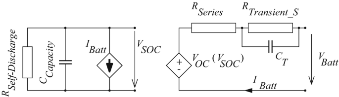
Battery model according to Chen et al. (simplified)
Let us consider the voltage which is available at the battery terminals when the current through these terminals is zero. The voltage at the battery terminals will typically non-linearly depend on V SOC. This dependency can be modeled by a non-linear function V OC(V SOC), representing the open terminal output voltage of the battery. This voltage decreases when the battery provides some current. For a constant discharging current, \(R_{Series}+R_{Transient\_S}\) models the corresponding voltage drop. For short current spikes, the decrease is determined by the value of R Series only, since C T will act as a buffer. When the current consumption increases, time constant \(R_{Transient\_S} * C_T\) determines the speed for the transition from only R Series causing the voltage drop to \(R_{Series}+R_{Transient\_S}\) causing the voltage drop. The original proposal by Chen et al. includes a second resistor/capacitor pair in order to model transient output voltage behavior more precisely. Overall, this model captures the impact of high output currents on the voltage, the non-linear dependency of the output voltage, and self-discharge reasonably well. Simpler versions of this model exist, i.e., ones that do not model all three effects.
-
Actual batteries exhibit the so-called charge recovery effect: whenever the discharge process of batteries is paused for some time interval, the battery recovers, i.e., more charge becomes available, and the voltage is typically also increased. This effect is not considered in Chen’s model. However, it is the focus of the so-called kinetic battery model (KiBaM) of Manwell et al. [364]. The name reflects the analogy upon which this model is based. The model assumes two different bins of charge, as shown in Fig. 3.64. The right bin contains the charge y 1 which is immediately available. The left bin contains charge y 2 which exists in the battery but which needs to flow into the right bin to become available. An interval of heavy usage of the battery may almost empty the right bin. It will then take some time for charge to become available again. The speed of the recovery process is determined by parameter k, the width of the pipe connecting the two bins. The details of the model (like the amount of charge flowing) reflect the physical situation of the bins. This model describes the charge recovery process with some reasonable precision but fails to describe transients and self-discharge as captured in Chen’s model. The kinetic model has an impact on how embedded systems should be used. For example, it has been demonstrated that it is beneficial to plan for intervals, during which wireless transmission is turned off [144].
Fig. 3.64 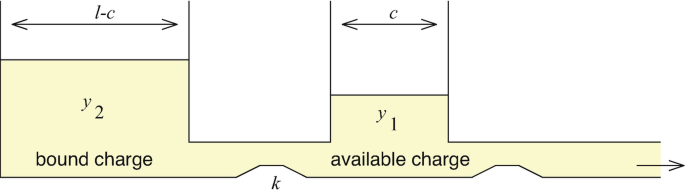
Kinetic battery model
Overall, the two models demonstrate nicely that models must be selected to reflect the effects that should be taken into account.
-
-
There may be mixed models which are partially based on abstract models and partially on chemical and physical models.


3.7.3 Energy Efficiency of Hardware Components
We will continue our discussion of energy efficiency by comparing the energy efficiency for the different technologies which we have at our disposal. Hardware components discussed in this chapter are quite different as far as their energy efficiency is concerned. A comparison between these technologies and changes over time (corresponding to a certain fabrication technology) can be seen in Fig. 3.65.Footnote 19 The figure reflects the conflict between efficiency and flexibility of currently available hardware technologies.

Hardware efficiency (ⒸDe Man and Philips)
The diagram shows the energy efficiency GOP/J in terms of number of operations per unit of energy of various target technologies as a function of time and the target technology. In this context, operations could be 32 bit additions. Obviously, the number of operations per joule is increasing as technology advances to smaller and smaller feature sizes of integrated circuits. However, for any given technology, the number of operations per joule is largest for hardwired application-specific integrated circuits (ASICs). For reconfigurable logic usually coming in the form of field programmable gate arrays (FPGAs; see p. 39), this value is about one order of magnitude less. For programmable processors, it is even lower. However, processors offer the largest amount of flexibility, resulting from the flexibility of software. There is also some flexibility for reconfigurable logic, but it is limited to the size of applications that can be mapped to such logic. For hardwired designs, there is no flexibility. The trade-off between flexibility and efficiency also applies to processors: for processors optimized for an application domain, such as processors optimized for digital signal processing (DSP), power-efficiency values approach those of reconfigurable logic. For general standard microprocessors, the values for this figure of merit are the worst. This can be seen from Fig. 3.65, comprising values for microprocessors such as ×86-like processors (see “MPU” entries), RISC processors, and the cell processor designed by IBM, Toshiba, and Sony.
Figure 3.65 does not identify exactly the applications which are compared, and it does not allow us to study the type of application mapping that has been performed.
More detailed and more recent comparisons have been made, enabling us to study the assumptions and the approach of these comparisons in a more comprehensive manner. A survey of comparisons involving GPUs has been published by Mittal et al. [398]. The survey includes a list of 28 publications for which GPUs have been found to be more energy-efficient than CPUs and 2 publications for which the reverse was true. Also, the survey comprises a list of 26 publications for which FPGAs have been found to be more energy-efficient than GPUs and 1 for which the reverse was true. For example, Hamada et al. [200] found for a gravitational n-body simulation that the number of operations per watt was by a factor of 15 higher for FPGAs than for GPUs. For a comparison against CPUs, the factor was 34. The exact factors certainly depend on the application, but as a rule of thumb, we can state the following: If we aim at top power- and energy-efficient designs, we should use ASICs. If we cannot afford ASICs, we should go for FPGAs. If FPGAs are also not an option, we should select GPUs. Also, we have already seen that heterogeneous processors are in general more energy-efficient than homogeneous processors. More detailed information can be computed for particular application areas.
3.7.3.1 The Case of Mobile Phones
Among the different applications of embedded systems (see pp. 4–8), we are now looking at telecommunication and smart phones. For smart phones, computational requirements are increasing at a rapid rate, especially for multimedia applications. De Man and Philips estimated that advanced multimedia applications need about 10–100 billion operations per second. Figure 3.65 demonstrates that advanced hardware technologies provided us more or less with this number of operations per joule (= Ws) in 2007. This means that the most power -efficient platform technologies hardly provided the efficiency which was needed. Standard processors (entries for MPU and RISC) were hopelessly inefficient. It also meant that all sources of efficiency improvements needed to be exploited. More recently, the power efficiency has been improved. However, all such improvements are typically compensated by trends to provide a higher quality, e.g., by an increase of the resolution of still and moving images as well as a higher bandwidth for communication.
A detailed analysis of the power consumption has been published by Berkel [553] and by Carroll et al. [84]. A more recent analysis including LTE mobile phones has been published by Dusza et al. [144]. A power consumption of up to around 4 watts has been observed. The display itself caused a consumption of up to around 1 watt, depending on the display brightness.
Improving battery technology would allow us to consume power over longer periods, but the thermal limitation prevents us from going significantly beyond the current consumption in the near future. Due to thermal issues, it has become standard to design mobile phones with temperature sensors and to throttle devices in case of overheating. Of course, a larger power consumption would be feasible for larger devices. Nevertheless, environmental concerns also result in the need to keep the power consumption low.
Technology forecasts have been published as so-called International Technology Roadmap for Semiconductors. In the ITRS edition of 2013 [261], it is explicitly stated that mobile phones are driving technological development: “System integration has shifted from a computational, PC-centric approach to a highly diversified mobile communication approach. The heterogeneous integration of multiple technologies in a limited space (e.g., GPS, phone, tablet, mobile phones, etc.) has truly revolutionized the semiconductor industry by shifting the main goal of any design from a performance driven approach to a reduced power driven approach. In few words, in the past performance was the one and only goal; today minimization of power consumption drives IC design.”
3.7.3.2 Sensor Networks
Sensor networks used for the Internet of Things are another special case. For sensor networks, there may be even much less energy available than for mobile phones. Hence, energy efficiency is of utmost importance, comprising of course energy-efficient communication [543].
3.8 Secure Hardware
The general requirements for embedded systems can often include security (see p. 9). In particular, security is important for the Internet of Things. If security is a major concern, special secure hardware may need to be developed. Security may need to be guaranteed for communication and for storage [309]. Security has to be provided despite possible attacks and countermeasures must be designed. Attacks can be partitioned into the following [300]:
-
Software attacks are based on the execution of software. The deployment of software Trojans is an example of such an attack. Also, software defects can be exploited. Buffer overflows are a frequent cause of security hazards. Side-channel attacks try to exploit additional sources of information complementing the specified interfaces. Side-channel attacks based on software execution are difficult, but not infeasible. For example, it may be possible to exploit execution time information.Footnote 20 Security-relevant algorithms should be designed such that their execution time does not depend on data values. This requirement also affects the implementation of computer arithmetic: instructions should not have data-dependent execution times.
-
Attacks which require physical access and which can be classified into the following:
-
Physical attacks try to open a side channel by physically tampering with the system. For example, silicon chips can be opened and analyzed. The first step in this procedure is de-packaging (removing the plastic covering the silicon). Next, micro-probing or optical analysis can be used. Such attacks are difficult, but they reveal many details of the chip.
-
Power analysis is another class of attacks. Power analysis techniques include simple power analysis (SPA) and differential power analysis (DPA). In some cases, SPA may be sufficient to compute encryption keys. In other cases, advanced statistical methods may be needed to directly compute keys from small statistical fluctuations of measured currents.
-
Analysis of electromagnetic radiation is another class of side-channel attacks.
-
Different classes of people might try these attacks, and different classes of people may have an interest in blocking these attacks. The attacker may actually be the user of an embedded device trying to obtain unauthorized network access or unauthorized access to protected media such as music.
We can distinguish between the following countermeasures:
-
A security-aware software development process is required as a shield against software attacks.
-
Tamper-resistant devices include special mechanisms for physical protection (shielding, or sensors to detect tampering with the modules).
-
Devices can be designed such that processed data patterns have very little impact on the power consumption. This requires special devices which are typically not used in complex chips.
-
Logical security, typically provided by cryptographic methods: encryption can be based on either symmetric or asymmetric ciphers.
-
For symmetric ciphers, sender and receiver are using the same secret key to encrypt and decrypt messages. DES, 3DES, and AES are examples of symmetric ciphers.
-
For asymmetric ciphers, messages are encrypted with a public key and decrypted with a private key. RSA and Diffie-Hellman are examples of asymmetric ciphers.
-
Also, hash codes can be added to messages, allowing the detection of message modifications. MD5 and SHA are examples of hashing algorithms.
Due to the performance gap, some processors may support encryption and decryption with dedicated instructions. Also, specialized solutions such as ARM’s TrustZone computing exist. “At the heart of the TrustZone approach is the concept of secure and non-secure worlds that are hardware separated, with non-secure software blocked from accessing secure resources directly. Within the processor, software either resides in the secure world or the non-secure world; a switch between these two worlds is accomplished via software referred to as the secure monitor (Cortex-A) or by the core logic (Cortex-M). This concept of secure (trusted) and non-secure (non-trusted) worlds extends beyond the processor to encompass memory, software, bus transactions, interrupts, and peripherals within an SoC” (see https://www.arm.com/products/security-on-arm/trustzone).
The Kalray MPPA2® -256 multi-core processor chip contains as many as 128 specialized crypto co-processors connected to a matrix of 288 “regular” cores (see http://www.kalrayinc.com/kalray/products/). Cores are 64 bit VLIW processors.
-
The following challenges exist for the design of countermeasures [300]:
-
1.
Performance gap: Due to the limited performance of embedded systems, advanced encryption techniques may be too slow, in particular if high data rates have to be processed.
-
2.
Battery gap: Advanced encryption techniques require a significant amount of energy. This energy may be unavailable in a portable system. Smart cards are a special case of hardware that must run using a very small amount of energy.
-
3.
Lack of flexibility: Frequently, many different security protocols are required within one system, and these protocols may have to be updated from time to time. This hinders using special hardware accelerators for encryption.
-
4.
Tamper resistance: Mechanisms against malicious attacks need to be built in. Their design is far from trivial. For example, it may be difficult if not impossible to guarantee that the current consumption is independent of the cryptographic keys that are processed.
-
5.
Assurance gap: The verification of security requires extra efforts during the design.
-
6.
Cost: Higher security levels increase the cost of the system.
Ravi et al. have analyzed these challenges in detail for a Secure Sockets Layer (SSL) protocol [300].
More information on secure hardware is available, for example, in a book by Gebotys [180] and in proceedings of a workshop series dedicated to this topic (see [183] for the most recent edition).
3.9 Problems
We suggest solving the following problems either at home or during a flipped classroom session:
3.1
It is suggested that locally available small robots are used to demonstrate hardware in the loop, corresponding to Fig. 3.2. The robots should include sensors and actuators. Robots should run a program implementing a control loop. For example, an optical sensor could be used to let a robot follow a black line on the ground. The details of this assignment depend on the availability of robots.
3.2
Define the term “signal”!
3.3
Which circuit do we need for the transition from continuous time to discrete time?
3.4
What does the sampling theorem tell us?
3.5
Assume that we have an input signal x consisting of the sum of sine waves of 1.75 kHz and 2 kHz. We are sampling x at a rate of 3 kHz. Will we be able to reconstruct the original signal after discretization of time? Please explain your result!
3.6
Discretization of values is based on ADCs. Develop the schematic of a flash-based ADC for positive and negative input voltages! The output should be encoded as 3 bit two’s complement numbers, allowing to distinguish between eight different voltage intervals.
3.7
Suppose that we are working with a successive approximation-based 4 bit ADC. The input voltage range extends from V min =1 V (="0000") to V max =4.75 V (="1111"). Which steps are used to convert voltages of 2.25 V, 3.75 V, and 1.8 V? Draw a diagram similar to Fig. 3.12 which depicts the successive approximation to these voltages!
3.8
Compare the complexity of flash-based and successive approximation-based ADC. Assume that you would like to distinguish between n different voltage intervals. Enter the complexity into Table 3.2, using the \({\mathcal {O}}\)-notation.
3.9
Suppose a sine wave is used as an input signal to the converter designed in Problem 3.6. Depict the quantization noise signal for this case!
3.10
Create a list of features of DSP processors!
3.11
Which components do FPGAs comprise? Which of these are used to implement Boolean functions? How are FPGAs configured? Are FPGAs energy-efficient? Which kind of applications are FPGAs good for?
3.12
What is the key idea of VLIW processors?
3.13
What is a “single-ISA heterogeneous multi-core architecture”? Which advantages do you see for such an architecture?
3.14
Explain the terms “GPU” and “MPSoC”!
3.15
Some FPGAs support an implementation of all Boolean functions of six variables. How many such functions exist? We ignore that some functions differ only by a renaming of variables.
3.16
In the context of memories, we are sometimes saying “small is beautiful.” What could be the reason for this?
3.17
Some levels of the memory hierarchy may be hidden from the application programmer. Why should such a programmer nevertheless care about the architecture of such levels?
3.18
What is a “scratchpad memory” (SPM)? How can we ensure that some memory object is stored in the SPM?
3.19
Develop the following FlexRay™ cluster: The cluster consists of the five nodes A, B, C, D, and E. All nodes should be connected via two channels. The cluster uses a bus topology. The nodes A, B, and C are executing a safety critical task, and therefore their bus requests should be guaranteed at the time of 20 macroticks. The following is expected from you:
-
Download the levi FlexRay simulator [495]. Unpack the ZIP file and install!
-
Start the training module by executing the file leviFRP.jar.
-
Design the described FlexRay cluster within the training module.
-
Configure the communication cycle such that the nodes A, B, and C have a guaranteed bus access within a maximal delay of 20 macroticks. The nodes D and E should use only the dynamic segment.
-
Configure the node bus requests. The node A sends a message every cycle. The nodes B and C send a message every second cycle. The node D sends a message of the length of 2 minislots every cycle, and the node E sends every second cycle a message of the length of 2 minislots.
-
Start the visualization and check if the bus requests of the nodes A, B, and C are guaranteed.
-
Swap the positions of nodes D and E in the dynamic segment. What is the resulting behavior?
3.20
Develop the schematic of a 3 bit DAC! The conversion should be done for a 3 bit vector x encoding positive numbers. Prove that the output voltage is proportional to the value represented by the input vector x. How would you modify the circuit if x represented two’s complement numbers?
3.21
The circuit shown in Fig. B.4 in Appendix B is an amplifier, amplifying input voltage V 1:
Compute the gain g closed for the circuit of Fig. B.4 as a function of R and R 1!
3.22
How do different hardware technologies differ with respect to their energy efficiency?
3.23
The computational efficiency is sometimes also measured in terms of billions of operations per second per watt. How is this different from the figure of merit used in Fig. 3.65?
3.24
Why is it so important to optimize embedded systems? Compare different technologies for processing information in an embedded system with respect to their efficiency!
3.25
Suppose that your mobile phone uses a lithium battery rated at 720 mAh. The nominal voltage of the battery is 3.7 V. Assuming a constant power consumption of 1 W, how long would it take to empty the battery? All secondary effects such as decreasing voltages should be ignored in this calculation.
3.26
Which challenges do you see for the security of embedded systems?
3.27
What is a “side-channel attack”? Please provide examples of side-channel attacks!
Notes
- 1.
This presentation is based on the assumption that a comprehensive coverage of Fourier approximations cannot be included in our course. Therefore, only the impact of these approximations is demonstrated by examples. Knowing the theory behind these examples would be beneficial (see, e.g., http://www.dspguide.com).
- 2.
This would require knowing the signal to be filtered for an infinite amount of time.
- 3.
In practice, the case of equal voltages is not relevant, as the actual behavior for very small differences between the voltages at the two inputs depends on many factors (like temperatures, manufacturing processes, etc.) anyway.
- 4.
Such encoders are also useful for finding the most significant ’1’ in the mantissa of floating-point numbers.
- 5.
Fortunately, the conversion from digital-to-analog values (D/A conversion) can be implemented very efficiently and can be very fast (see p. 54).
- 6.
This can be done with a capacitor in the feedback loop of an operational amplifier (see p. 397).
- 7.
In 2017, http://anysilicon.com/semiconductor-wafer-mask-costs/ mentioned an average cost of about $ 1.5M for a 28 nm technology.
- 8.
In practice, the increase may actually come with a larger exponential.
- 9.
The availability of large flash memories and 3D integration make memory size constraints less tight.
- 10.
We continue denoting multiplexers, arithmetic units, and memories by shape symbols, due to their widespread use in technical documentation. For memories, we adopt shape symbols including an explicit address decoder (included in the shape symbols for the ROMs on the right). These decoders identify the address input.
- 11.
Instructions using predicated execution have an effect only if a certain condition encoded in the instruction evaluates to true. This condition typically involves values stored in condition code registers, resulting from previous instructions. For example, instructions might have an effect only if a previous <= -expression was true. Predication can be used to implement if statements efficiently: the condition is stored in one of the condition registers, and if-statement bodies are implemented as predicated instructions which depend on this condition. For ARM processors, the condition is encoded in the first 4 bits of the instruction format. As a special case, an “always” condition can be encoded, like in Fig. 3.19. The more recently introduced 64 bit instruction set places less emphasis on predicated execution.
- 12.
Using VHDL notation (see p. 70), concatenation is denoted by an & sign, and constants are enclosed in quotes in Fig. 3.19.
- 13.
In our notation, a 0 is the weight of the oldest input value. If we would define a 0 as the weight of the youngest value of w, the first term would take the more commonly used form w s−k. Our notation simplifies understanding the program code shown below.
- 14.
See Appendix C on p. 401 for an introduction to paging.
- 15.
Rotation of this figure would improve its readability but would contradict the official designation of this layout style.
- 16.
In fact, it is frequently difficult to select the right parameters.
- 17.
In practice, due to rise and fall times being > 0, transitions from one step to the next will not be ideal, but take some time.
- 18.
Reconstruction may be possible if additional information about the signal is available, e.g., if we restrict ourselves to certain signal types.
- 19.
The figure approximates information provided by H. De Man [363] and is based on information provided by Philips.
- 20.
Side-channel attacks based on timing information have been published under the names Spectre and Meltdown. They apply to modern processors using speculative execution; see https://en.wikipedia.org/wiki/Spectre_(security_vulnerability).
References
Aamodt, T., Chow, P.: Embedded ISA support for enhanced floating-point to fixed-point ANSI C compilation. In: Proceedings of the International Conference on Compilers, Architectures, and Synthesis for Embedded Systems (CASES), pp. 128–137 (2000)
Absint: aiT worst-case execution time analyzers (2020). http://www.absint.de/ait
Analog Devices Inc. Eng.: ADSP-2100 Family User’s Manual. Out of print (1995)
Analog Devices Inc. Eng.: Data Conversion Handbook (Analog Devices). Newnes, London (2004)
ARM Ltd.: AMBA specifications (2020). http://www.arm.com/products/system-ip/amba-specifications.php
ARM Ltd.: big.LITTLE Technology (2020). http://www.arm.com/products/processors/technologies/biglittleprocessing.php
ARM Ltd.: Mali-T860 & Mali-T880 (2020). http://www.arm.com/products/multimedia/mali-gpu/high-performance/mali-t860-t880.php
Atmel: 32-Bit AVR Microcontroller (2012). http://www.atmel.com/Images/doc32058.pdf
Banakar, R., Steinke, S., Lee, B.S., Balakrishnan, M., Marwedel, P.: Scratchpad memory: A design alternative for cache on-chip memory in embedded systems. In: Proceedings of the International Symposium on Hardware-Software Codesign (CODES), pp. 73–78 (2002). http://doi.acm.org/10.1145/774789.774805
Benini, L., Bogliolo, A., De Micheli, G.: A survey of design techniques for system-level dynamic power management. IEEE Trans. VLSI Syst. 8(3), 299–316 (2000)
Beszedes, A.: Survey of code size reduction methods. ACM Comput. Surv. 35, 223–267 (2003)
Bonny, T., Henkel, J.: Huffman-based code compression techniques for embedded processors. ACM Trans. Des. Autom. Electron. Syst. 15(4), 31:1–31:37 (2010). https://doi.org/10.1145/1835420.1835424. http://doi.acm.org/10.1145/1835420.1835424
Burd, T., Brodersen, R.: Design issues for dynamic voltage scaling. In: International Symposium on Low Power Electronics and Design (ISLPED), pp. 9–14 (2000)
Burd, T., Brodersen, R.W.: Energy efficient microprocessor design. Kluwer Academic Publishers, Dordrecht (2003)
Burks, A., Goldstine, H., von Neumann, J.: Preliminary discussion of the logical design of an electronic computing element. Report to U.S. Army Ordnance Department (1946). Reprinted at https://www.cs.princeton.edu/courses/archive/fall10/cos375/Burks.pdf
Carroll, A., Heiser, G.: An analysis of power consumption in a smartphone. In: Proceedings of the 2010 USENIX Conference on USENIX Annual Technical Conference, USENIXATC’10, pp. 21–21. USENIX Association, Berkeley (2010). http://dl.acm.org/citation.cfm?id=1855840.1855861
Chandrakasan, A.P., Sheng, S., Brodersen, R.W.: Low-power CMOS digital design. IEEE J. Solid-State Circuits 27(4), 119–123 (1992)
Chao, C., Saeta, B.: HotChips 2019 Tutorial – Cloud TPU: Codesigning Architecture and Infrastructure (2019). https://www.hotchips.org/hc31/HC31_T3_Cloud_TPU_Codesign.pdf
Chen, M., Rincón-Mora, G.: Accurate electrical battery model capable of predicting runtime and i-v performance. IEEE Trans. Energy Convers. 21, 504–511 (2006)
Chiu, Y.: Folding and Interpolating ADC. University of Texas at Dallas, EECT 7327 (2014). http://www.utdallas.edu/~yxc101000/courses/7327/slides/intp%20folding%20adc.pptx
Dasgupta, S.: The organization of microprogram stores. ACM Comput. Surv. 11, 39–65 (1979)
Drepper, U.: What every programmer should know about memory (2007). http://www.akkadia.org/drepper/cpumemory.pdf
Dusza, B., Marwedel, P., Spinczyk, O., Wietfeld, C.: A context-aware battery lifetime model for carrier aggregation enabled LTE-A systems. In: IEEE Consumer Communications and Networking Conference (CCNC) (2014)
Elsevier B.V.: Sensors and actuators A: physical. An Int. J. (2020)
Elsevier B.V.: Sensors and actuators B: chemical. An Int. J. (2020)
Flautner, K.: Heterogeneity to the rescue (2011). https://www.bscmsrc.eu/sites/default/files/media/arm-heterogenous-mp-november-2011.pdf
Freescale Semiconductor/NXP: ColdFire® Family Programmer’s Reference Manual (2005). http://www.nxp.com/assets/documents/data/en/reference-manuals/CFPRM.pdf
Gebotys, C.: Security in Embedded Devices. Springer, Berlin (2010)
Gierlichs, B., Poschmann, A.: International Workshop on Cryptographic Hardware and Embedded Systems (CHES) (2016). http://www.chesworkshop.org/
Goldberg, D.: What every computer scientist should know about floating point arithmetic. ACM Comput. Surv. 23, 5–48 (1991)
Goodfellow, I., Bengio, Y., Courville, A.: Deep Learning. MIT Press, Cambridge (2016)
Hamada, T., Benkrid, K., Nitadori, K., Taiji, M.: A comparative study on ASIC, FPGAs, GPUs and general purpose processors in the O(N 2) gravitational N-body simulation. In: Proceedings of the 2009 NASA/ESA Conference on Adaptive Hardware and Systems, AHS ’09, pp. 447–452. IEEE Computer Society, Washington (2009). https://doi.org/10.1109/AHS.2009.55. http://dx.doi.org/10.1109/AHS.2009.55
Hastie, T., Tibshirani, R., Friedman, R.: The Elements of Statistical Learning: Data Mining, Inference, and Prediction. Springer, Berlin (2009)
Hattori, T.: MPSoC approaches for low-power embedded SoC’s (2007). http://www.mpsoc-forum.org/previous/2007/slides/Hattori.pdf. http://www.mpsoc-forum.org/2007/slides/Hattori.pdf
Hennessy, J.L., Patterson, D.A.: Computer Architecture: A Quantitative Approach, 5th edn. Morgan Kaufmann, Burlington (2011)
Hunt, V.D., Puglia, A., Puglia, M.: RFID: A Guide to Radio Frequency Identification. Wiley, Hoboken (2007)
Intel: Enhanced Intel® SpeedStep® Technology for the Intel® Pentium® M Processor - White paper (2004). ftp://download.intel.com/design/network/papers/30117401.pdf
Intel: Motion estimation with Intel® streaming SIMD extensions 4 (Intel® SSE4) (2008). http://software.intel.com/en-us/articles/motion-estimation-with-intel-streaming-simd-extensions-4-intel-sse4
Intel: Intel® AVX (2010). http://software.intel.com/en-us/avx
Intel: Intel Itanium processor family (2016). http://www.intel.com/itcenter/products/itanium
ISO: Road vehicles - FlexRay communications system – Part 1: General information and use case definition (2013). http://www.iso.org/iso/home/store/catalogue_tc/catalogue_detail.htm?csnumber=59804
ITRS Organization: International Technology Roadmap for Semiconductors – 2013 Edition – Executive Summary (2013). http://www.itrs2.net/2013-itrs.html
Iyer, A., Marculescu, D.: Power and performance evaluation of globally asynchronous locally synchronous processors. In: International Symposium on Computer Architecture (ISCA), pp. 158–168 (2002)
Jouppi, N., Young, C., Patil, N., Patterson, D.: A domain-specific architecture for deep neural networks. Commun. ACM 61, 50–59 (2018). https://doi.org/10.1145/3154484
Khorramabadi, H.: ADC Converters - Pipelined ADCs. UC Berkeley, EECS 247, Lecture 22 (2005). http://www-inst.eecs.berkeley.edu/~ee247/fa05/lectures/L22_f05.pdf
Khorramabadi, H.: Oversampled ADCs. UC Berkeley, EECS 247, Lecture 23 (2009). http://www-inst.eecs.berkeley.edu/~ee247/fa05/lectures/L22_f05.pdf
Klaiber, A.: The technology behind Crusoe™ processors (2000). http://web.archive.org/web/20010602205826/www.transmeta.com/crusoe/download/pdf/crusoetechwp.pdf
Kocher, P., Lee, R., McGraw, G., Raghunathan, A.: Security as a new dimension in embedded system design. In: Proceedings of the 41st Annual Design Automation Conference, DAC ’04, pp. 753–760. ACM, New York (2004). Moderator-Ravi, Srivaths. https://doi.org/10.1145/996566.996771. http://doi.acm.org/10.1145/996566.996771
Koopman, P.J., Upender, B.P.: Time division multiple access without a bus master. United Technologies Research Center, UTRC Technical Report RR-9500470 (1995). http://www.ece.cmu.edu/~koopman/jtdma/jtdma.html
Kopetz, H., Grunsteidl, G.: TTP — a protocol for fault-tolerant real-time systems. IEEE Comput. 27, 14–23 (1994)
Krhovjak, J., Matyas, V.: Secure hardware - pv018 (2006). http://www.fi.muni.cz/~xkrhovj/lectures/2006_PV018_Secure_Hardware_slides.pdf
Kumar, R., Farkas, K.I., Jouppi, N.P., Ranganathan, P., Tullsen, D.M.: Single-ISA heterogeneous multi-core architectures: The potential for processor power reduction. In: Proceedings of the 36th Annual IEEE/ACM International Symposium on Microarchitecture, MICRO 36, pp. 81–. IEEE Computer Society, Washington (2003). http://dl.acm.org/citation.cfm?id=956417.956569
Lang, F.: A/D-converter for high-speed communication (in German). Ph.D. Thesis, Fakultät Informatik, Elektrotechnik und Informationstechnik der Universität Stuttgart (2014)
Latendresse, M.: The code compression bibliography (2004). http://www.iro.umontreal.ca/~latendre/compactBib
Li, Z.R. (ed.): Organic Light-Emitting Materials and Devices. CRC Press, Boca Raton (2015)
LIN Consortium: LIN Specification Package - Revision 2.2A (2010). http://www.cs-group.de/fileadmin/media/Documents/LIN_Specification_Package_2.2A.pdf
Machanik, P.: Approaches to addressing the memory wall. Technical Report, November, University Brisbane (2002)
Macii, E. (ed.): Ultra Low-Power Electronics and Design. Springer, Berlin (2004)
Macii, A., Benini, L., Poncino, M.: Memory Design Techniques for Low Energy Embedded Systems. Kluwer Academic Publishers, Dordrecht (2002)
Man, H.D.: From the heaven of software to the hell of nanoscale physics: an industry in transition. Keynote, HiPEAC ACACES Summer School, L’Aquila (2007)
Manwell, J.F., McGowan, J.G.: Lead acid battery storage model for hybrid energy systems. Sol. Energy 50, 399–405 (1993)
Meena, J.S., Sze, S.M., Chand, U., Tseng, T.Y.: Overview of emerging nonvolatile memory technologies. Nanoscale Res. Lett. 9(1), 526 (2014). https://doi.org/10.1186/1556-276X-9-526. http://dx.doi.org/10.1186/1556-276X-9-526
Mittal, S., Vetter, J.S.: A survey of methods for analyzing and improving GPU energy efficiency. ACM Comput. Surv. 47(2), 19:1–19:23 (2014). https://doi.org/10.1145/2636342. http://doi.acm.org/10.1145/2636342
MOST Cooperation: MOST Worldwide (2010). http://www.mostcooperation.com/
Moynihan, T.: CMOS is winning the camera sensor battle, and here’s why (2011). http://www.techhive.com/article/246931/cmos_is_winning_the_camera_sensor_battle_and_heres_why.html?page=0
Oliveira, D.L., Faria, L.A., Delsoto, H.A., Garcia, K.: An architecture for globally-synchronous locally-asynchronous systems on FPGAs. In: IEEE XXIII International Congress on Electronics, Electrical Engineering and Computing (INTERCON), pp. 1–6 (2016)
O’Neill, A.: Analog to digital types. IEEE TV (for members only) (2006). https://ieeetv.ieee.org/conference-highlights/analog-to-digital-types?
Oppenheim, A.V., Schafer, R., Buck, J.R.: Digital Signal Processing. Pearson Higher Education, New York (2009)
Patterson, D.: Domain-Specific Architectures for Deep Neural Networks (2019). https://inst.eecs.berkeley.edu//~cs152/sp19/lectures/L20-DSA.pdf
Peukert, W.: Über die Abhängigkeit der Kapacität von der Entladestromstärcke bei Bleiakkumulatoren. Elektrotechnische Zeitschrift, vol. 20 (1897)
Piatkowski, N.: Exponential families on resource-constrained systems. Ph.D. Thesis, TU Dortmund University, Dortmund (2018). URL https://eldorado.tu-dortmund.de/handle/2003/36877
Rao, R., Vrudhula, S., Rakhmatov, D.: Battery modeling for energy-aware system design. IEEE Comput. 36, 77–87 (2003)
Rixner, S., Dally, W.J., Khailany, B.J., Mattson, P.J., Kapasi, U.J.: Register organization for media processing. In: 6th High-Performance Computer Architecture (HPCA-6), pp. 375–386 (2000)
Sarajlic, E., Yamahata, C., Cordero, M., Fujita, H.: Three-phase electrostatic rotary stepper micromotor with a flexural pivot bearing. J. Microelectromech. Syst. 19(2), 338–349 (2010). https://doi.org/10.1109/JMEMS.2010.2040139
Science X: Imec reports breakthrough power efficiency and performance of coarse-grain processor (2005). https://phys.org/news/2005-11-imec-breakthrough-power-efficiency-coarse-grain.html
SGI: OpenGL software development kit (2016). https://www.opengl.org/sdk/libs/
Siciliano, B., Oussama, O.: Handbook of Robotics. Springer, Berlin (2016)
Sirocic, B., Marwedel, P.: Levi Flexray® simulation software (2007). https://ls12-www.cs.tu-dortmund.de/daes/media/documents/teaching/downloads/levi/download/leviFRP.zip
Society for Display Technology: Home page (2003). http://www.sid.org
Stritter, E., Gunter, T.: Microprocessor architecture for a changing world: The Motorola 68000. IEEE Comput. 12, 43–52 (1979)
Texas Instruments Inc.: 66AK2x Multicore DSP + ARM Processors (2016). http://www.ti.com/lsds/ti/processors/dsp/c6000_dsp-arm/66ak2x/overview.page
The Dobelle Institute: Home page (2003). http://www.dobelle.com (no longer accessible)
Tian, T., Shih, C.P.: Software techniques for shared-cache multi-core systems (2012). https://software.intel.com/en-us/articles/software-techniques-for-shared-cache-multi-core-systems
Tiwari, A., Ballal, P., Lewis, F.L.: Energy-efficient wireless sensor network design and implementation for condition-based maintenance. ACM Trans. Sen. Netw. 3(1), 1-es (2007). https://doi.org/10.1145/1210669.1210670. http://doi.acm.org/10.1145/1210669.1210670
Vahid, F.: Procedure exlining. In: Proceedings of the International Symposium on System Synthesis (ISSS), pp. 84–89 (1995)
van Berkel, C.H.K.: Multi-core for mobile phones. In: Proceedings of the Conference on Design, Automation and Test in Europe, DATE ’09, pp. 1260–1265. European Design and Automation Association, 3001 Leuven, Belgium (2009). http://dl.acm.org/citation.cfm?id=1874620.1874924
Vogels, M., Gielen, G.: Architectural selection of A/D converters. In: Proceedings of the Design Automation Conference (DAC), pp. 974–977 (2003). https://doi.org/10.1145/775832.776076. http://doi.acm.org/10.1145/775832.776076
Wainwright, M.J., Jordan, M.I.: Graphical models, exponential families, and variational inference. Found. Trends Mach. Learn. 1(1–2), 1–305 (2008). http://dx.doi.org/10.1561/2200000001
Weddell, A.S., Magno, M., Merrett, G.V., Brunelli, D., Al-Hashimi, B.M., Benini, L.: A survey of multi-source energy harvesting systems. In: Proceedings of the Conference on Design, Automation and Test in Europe, DATE ’13, pp. 905–908. EDA Consortium, San Jose (2013). http://dl.acm.org/citation.cfm?id=2485288.2485505
Wikipedia: Aircraft principal axes (2020). https://en.wikipedia.org/wiki/Aircraft_principal_axes
Wikipedia: Energy harvesting (2020). https://en.wikipedia.org/wiki/Energy_harvesting
Wilton, S., Jouppi, N.: CACTI: An enhanced access and cycle time model. Int. J. Solid State Circ. 31(5), 677–688 (1996)
Wolf, W.: Computers as Components. Morgan Kaufmann, Burlington (2001)
Xilinx: MicroBlaze processor reference guide (2008). http://www.xilinx.com/support/documentation/sw_manuals/mb_ref_guide.pdf
Xilinx Inc.: UltraScale Architecture Configurable Logic Block (2015). http://www.xilinx.com/support/documentation/user_guides/ug574-ultrascale-clb.pdf
Xilinx Inc.: UltraScale+ FPGAs - Product Tables and Product Selection Guide (2016). http://www.xilinx.com/support/documentation/selection-guides/ultrascale-plus-fpga-product-selection-guide.pdf
Xilinx Inc.: UltraScale Architecture and Product Overview (2016). http://www.xilinx.com/support/documentation/data_sheets/ds890-ultrascale-overview.pdf
Author information
Authors and Affiliations
Rights and permissions
Open Access This chapter is licensed under the terms of the Creative Commons Attribution 4.0 International License (http://creativecommons.org/licenses/by/4.0/), which permits use, sharing, adaptation, distribution and reproduction in any medium or format, as long as you give appropriate credit to the original author(s) and the source, provide a link to the Creative Commons license and indicate if changes were made.
The images or other third party material in this chapter are included in the chapter's Creative Commons license, unless indicated otherwise in a credit line to the material. If material is not included in the chapter's Creative Commons license and your intended use is not permitted by statutory regulation or exceeds the permitted use, you will need to obtain permission directly from the copyright holder.
Copyright information
© 2021 The Author(s)
About this chapter

Cite this chapter
Marwedel, P. (2021). Embedded System Hardware. In: Embedded System Design. Embedded Systems. Springer, Cham. https://doi.org/10.1007/978-3-030-60910-8_3
Download citation
DOI: https://doi.org/10.1007/978-3-030-60910-8_3
Published:
Publisher Name: Springer, Cham
Print ISBN: 978-3-030-60909-2
Online ISBN: 978-3-030-60910-8
eBook Packages: EngineeringEngineering (R0)