
Abstract
OTP (One Time Programmable) memory in power technology enables electrical performance optimization together with area occupation reduction. In this paper, the aspects relative to the oxide breakdown (which is the key mechanism for memory programmability) are studied and applied to the development of an antifuse OTP cell in a 350 nm-CMOS power technology. The physical analysis of the degradation phases of an oxide layer is presented together with the physical models, exploited to foresee the device time-to-breakdown depending on applied voltage, oxide thickness etc. The achieved results are used in the development and reliable implementation of OTP cells in the target 350 nm-CMOS node.
Zusammenfassung
OTP-Speicher (One Time Programmable) in der Energietechnik ermöglicht die Optimierung der elektrischen Leistung bei gleichzeitiger Reduzierung der Flächenbelegung. In diesem Beitrag werden die Aspekte in Bezug auf den Oxiddurchbruch (welcher der Schlüsselmechanismus für die Programmierbarkeit des Speichers ist) untersucht und auf die Entwicklung einer OTP-Zelle mit Antifuse-Funktion in einer 350nm-CMOS-Leistungstechnologie angewandt. Die physikalische Analyse der Degradationsphasen einer Oxidschicht wird zusammen mit den physikalischen Modellen vorgestellt, die ausgenutzt werden, um die Zeit bis zum Durchbruch des Bauelements in Abhängigkeit von der angelegten Spannung, Oxiddicke usw. vorherzusehen. Die erzielten Ergebnisse werden bei der Entwicklung und zuverlässigen Implementierung von OTP-Zellen im 350nm-CMOS-Zielknoten verwendet.
1 Introduction
Recently aggressive optimization of power devices is exploiting digital programmability, which is possible for the availability of on-chip low-cost memory as OTP (One Time Programmable) cells. Digital programmability is exploited in power devices to configure the circuit and optimize it for any operation condition. On the other hand, in the design of analog blocks, where the power devices are not specifically developed for, digital programmability is exploited to adjust and tune performance to achieve accuracy otherwise critical in such technology. This key need of on-chip memory in power technology is satisfied by the development of low-cost OTP cells, which have to guarantee efficient and reliable programmability mechanism.
In an OTP cell, the oxide is the antifuse element to be programmed by inducing its Breakdown reliability and within a certain time, defined Time-To-Breakdown (\(T_{BD}\)).
In this paper, the mechanisms producing the Breakdown events are presented and their effects are studied for the development of an OTP cell in 350 nm technology with 7.7 nm oxide thickness (\(t_{ox}\)).
2 Oxide degradation processes
The main classes of processes producing oxide degradation, resulting in damages and, then, in Breakdown are the Wearout currents and the Defect Generation Mechanisms, as described in the following.
2.1 Wearout currents
If a voltage is applied to an oxide layer, a leakage current flows, called tunneling or wearout current. There are two main mechanisms causing such current:
-
Fowler-Nordheim tunneling (FN): the band diagram deforms such that the electron crosses a triangular potential barrier. Such FN current is due to electrons reaching the anode passing through the oxide conduction band, as in Fig. 1(left), and is:
$$ J_{FN}= A \cdot {E_{ox}}^{2} \cdot \exp \big( - \frac{B}{E_{ox}} \big) $$(1)where \(q\) is the elementary charge, and \(A\), \(B\) parameters are:
$$ A= \frac{q^{3}}{8\pi h \phi _{e} } \cdot \frac{m^{*}_{Si}}{m^{*}_{ox}}\quad \text{and}\quad B= \frac{8 \pi \sqrt{2m^{*}_{ox}} \; {\phi _{e}}^{3/2}}{3hq} $$(2)with \(m^{*}_{Si}\) the electron rest mass, \(m^{*}_{ox}\) the electron effective mass within the dielectric and \(\phi _{e}\) the injecting electrode barrier height. FN mechanism dominates for high electric fields;
Fig. 1. 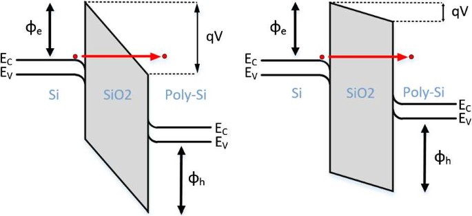
Energy band diagrams: Fowler-Nordheim (left) and Direct (right) Tunneling
-
Direct Tunneling (DT): the current is due to cathode injected electrons crossing a trapezoidal potential barrier (between metal/oxide/Si in CMOS) reaching the anode without flowing into the oxide conduction band as shown in Fig. 1(right). The approximated DT current is:
$$ J_{DT}= A \cdot {E_{ox}}^{2} \cdot \exp \Big(- \frac{B}{E_{ox}} \cdot \Big[ 1- {\Big( 1- \frac{V_{ox}}{\phi _{e}} \Big) }^{3/2} \Big] \Big) $$(3)This mechanism dominates for low electric fields;

For a given \(E_{ox}\), the DT current density is higher than the FN one. Based on the tunneling regime, differences in the Breakdown event, such as its rapidity, are to be expected.
The Electric field (\(E_{ox}\)) threshold between the DT and FN is between \(5-20\,{\mathrm{MV/cm}}\), e.g. for a \(t_{ox}=7.7\, {\mathrm{nm}}\) corresponds to \(\simeq 3.8\,{\mathrm{V}}\). For thick oxide (\(t_{ox}>5\,{\mathrm{nm}}\)) and electric fields above \(5-8\,{\mathrm{MV/cm}}\) FN current dominates [1]. While for thin oxide (\(t_{ox}<5\,{\mathrm{nm}}\)) and voltage below \(3.1-3.2\, {\mathrm{V}}\) (corresponding to the barrier height between n-doped silicon and SiO2) the DT dominates. Since \(E_{ox}=V_{G}/t_{ox}\), where \(V_{G}\) is the voltage applied across the gate oxide, any \(t_{ox}\) change would affect the MV/cm ratio. In the implementation of an OTP cell using 350 nm technology (\(t_{ox}=7.7\) nm) in high voltage (>10 V) domain, the \(E_{ox}\simeq 13\, {\mathrm{MV/cm}}\), therefore the FN current is expected to dominate.
2.2 Defect generation mechanisms
Defects in an oxide layer are due to fabrication imperfections and/or generation mechanisms. These defects would introduce traps or recombination centers into the forbidden \(SiO_{2}\) band-gap, which enable carriers to tunnel the oxide and, depending on their energies, to trigger other defect creation mechanisms. In a trap-assisted tunneling, considering a single trap, electrons tunnel from the cathode to the trap and then from the trap to the anode, as shown in Fig. 2 (left) for a deep (top) and an interface (bottom) trap.

Trap assisted tunneling (left), AHI mechanism (right)
For electrons with energy \(>5\,{\mathrm{eV}}\) [1], [2] (as it is the case for the higher voltages required in the OTP Breakdown) the Anode Hole Injection (AHI) mechanism and bonds rupture, shown in Fig. 2 (right), are activated. Hot electrons tunnel the triangular barrier reaching the anode conduction band. Then, they transfer their energy to deep valence-band electrons, which are promoted to the conduction band leaving holes behind. Due to \({E_{ox}}\), hot holes tunnel into oxide valence band. This could lead to interface traps generation and recombination centers for incoming electrons [8]. Trap assisted tunneling in localized spots follows, leading to irreversible oxide damages.
3 Breakdown physical models
The OTP programmability efficiency and reliability depends on the accuracy of the evaluation of \(T_{BD}\), whose value depends on the dominating defect creation mechanisms. There are three main mechanisms producing Breakdown, each of which leading to a different \(T_{BD}\).
-
E Model (also Thermo-Chemical model): the Breakdown results from the covalent \(SiO_{2}\) bonds rupture due to the electric field [7]. In this case:
$$ T_{BD,E}= (C \cdot e^{\frac{E_{a}}{K_{b} T}}) \cdot e^{- G \cdot E_{ox} } $$(4)where \(G\) is the electric field acceleration factor and \(E_{a}\) is the activation energy for the oxide Breakdown;
-
1/E Model (also AHI model): the Breakdown is due to the hot holes injected from the anode. The hole tunneling current can be expressed as the product between the electron FN tunneling current and a term expressing the probability of the hole generation and tunneling through the anode barrier [3], [4]. The amount of injected holes determines the \(T_{BD}\), expressed as:
$$ T_{BD,1/E}= (D \cdot e^{\frac{E_{a}}{K_{b} T}}) \cdot e^{ \frac{F}{E_{ox}} } $$(5) -
Power Law: linked to the hydrogen release phenomena. Hot tunneling electrons may break the Si-H bonds, leading to releasing of hydrogen atoms at the cathode interface. These can subsequently diffuse through the oxide and combine with oxygen vacancies [5]. In such a way, defects are generated till the Breakdown happens and \(T_{BD}\) is given by:
$$ T_{BD,\mathrm{Power}} = K\cdot {V_{G}}^{-\beta } $$(6)where \(\beta \) is the voltage acceleration factor [6], related to the disruption energy of Si-H bonds.
Depending on the implementation aspects (oxide quality, technology processes, electric field etc.) the relative importance of the three mechanisms changes and one of these could become dominating. The case with a 350 nm technology is discussed in the following section.
4 Models validation
Based on the above described physical mechanisms, the case of an OTP cell in the \(350\,{\mathrm{nm}}\) technology with oxide surface of 9.2 μm2 and thickness of \(7.7\,{\mathrm{nm}}\) is studied. The goal is to relate electric field, oxide properties and \(T_{BD}\). For this purpose, high voltage (>13 V) pulses are applied to the gate (while source and drain were shorted) to induce Breakdown. From Fig. 3, for \(13\,{\mathrm{V}}\) programming voltage, the Wearout current is about 50 μA and the \(T_{BD}\) is \(30\,{\mathrm{ms}}\). Since the electric field is \(>15\,{\mathrm{MV/cm}}\), the FN current dominates, as proven in Fig. 4 (left) where the Eq. (1) correctly fits the data. The extrapolated \(A\) and \(B\) parameters of Eq. (1) are:

Gate Current waveform for \(T_{BD}\) detection with a 13V-\(V_{G}\)

Wearout current fit with FN equation (left), \(T_{BD}\) fit (right)
The \(T_{BD}\) behaviour as a function of the applied voltage is shown in Fig. 4 (right). The fitting equations are (4), (5) and (6) where \(V_{g}/t_{ox} = E_{ox}\). The extrapolated parameters are:
These results are validated also by the good agreement with literature. In fact, \(B\) is consistent with [6] and E model parameters are comparable with those obtained in [7].
The fitting to the experimental data proves the pertinence of the three models. However, the experiment is yet not enough to determine which of those defect generation mechanisms have more impact. Indeed, breakdown is generally a consequence of more mechanisms superimposed. Anyway, guesses of \(T_{BD}\) can still be obtained by extrapolation. Must be pointed out that it is important to guarantee a maximum failure rate: the programmed oxide must be hardly broken, to avoid misunderstanding while reading the memory. The higher the electric field, the higher is the probability of having hard breakdowns in the programming time window. Nevertheless, producing a higher voltage would require more power and area consumption, affecting the overall chip cost. On the basis of these considerations, the specifications concerning the oxide properties, the target \(T_{BD}\) and the applied field are drawn and the OTP circuit design follows.
5 Conclusion
The paper explains the oxide Breakdown process in a high-voltage technology required for the development of an OTP cell. The main models and formulas, useful to relate the oxide lifetime with the oxide dimension and the applied field are presented. From the conducted experiments in the adopted 350 nm technology and in the range 13 to 16 V, the three mechanism results in similar \(T_{BD}\) and then \(T_{BD}\) optimization requires to manage all three phenomena. This validates the presented research activity. The same methodology can also be adopted for predicting the devices lifetime for the surrounding 350 nm CMOS circuit.
A part of the work has been performed in the project iDev40. The iDev40 project has received funding from the ECSEL Joint Undertaking (JU) under grant agreement No 783163. The JU receives support from the European Union’s Horizon 2020 research and innovation programme. It is co-funded by the consortium members, grants from Austria, Germany, Belgium, Italy, Spain and Romania. The information and results set out in this publication are those of the authors and do not necessarily reflect the opinion of the ECSEL Joint Undertaking.
References
Lombardo, S. A., Pey, K. L., Stathis, J., Palumbo, F. (2005): Dielectric breakdown mechanisms in gate oxides. J. Appl. Phys., 98, 121301.
DiMaria, D. J., Cartier, E. (1995): Mechanism for stress-induced leakage currents in thin silicon dioxide films. J. Appl. Phys., 78(6), 15.
Schuegraf, K. F., Hu, C. (1994): Hole injection SiO2 breadkown model for very low voltage lifetime extrapolation. IEEE Trans. Electron Devices, 41(5), 761–767.
Alam, M. A., Bude, J., Ghetti, A. (2000): Field acceleration for oxide breakdown – can an accurate anode hole injection model resolve the E vs. 1/E controversy?. In IEEE 38th annual international reliability physics symposium, San Jose, California.
Shluger, A. (2019): Defects in oxides in electronic devices. Handbook of materials modeling. Berlin: Springer.
Yang, C. H., Chen, S. C., Tsai, Y. S., Lu, R., Lee, Y.-H. (2017): The physical explanation of TDDB power law lifetime model through oxygen vacancy trap investigations in HKMG NMOS FinFET devices. New York: IEEE.
Fengming, L., Jiang, S., Xiaoyu, L., Xianghao, W. (2012): Validation test method of TDDB physics-of-failure models. In Prognostics & system health management conference.
Schuegraf, K. F., Hu, C. (1993): Hole injection oxide breakdown model for very low voltage lifetime extrapolation. In 31st annual proceedings reliability physics, Atlanta, USA.
Funding
Open access funding provided by Università degli Studi di Milano - Bicocca within the CRUI-CARE Agreement.
Author information
Authors and Affiliations
Corresponding author
Additional information
Publisher’s Note
Springer Nature remains neutral with regard to jurisdictional claims in published maps and institutional affiliations.
Rights and permissions
Open Access Dieser Artikel wird unter der Creative Commons Namensnennung 4.0 International Lizenz veröffentlicht, welche die Nutzung, Vervielfältigung, Bearbeitung, Verbreitung und Wiedergabe in jeglichem Medium und Format erlaubt, sofern Sie den/die ursprünglichen Autor(en) und die Quelle ordnungsgemäß nennen, einen Link zur Creative Commons Lizenz beifügen und angeben, ob Änderungen vorgenommen wurden. Die in diesem Artikel enthaltenen Bilder und sonstiges Drittmaterial unterliegen ebenfalls der genannten Creative Commons Lizenz, sofern sich aus der Abbildungslegende nichts anderes ergibt. Sofern das betreffende Material nicht unter der genannten Creative Commons Lizenz steht und die betreffende Handlung nicht nach gesetzlichen Vorschriften erlaubt ist, ist für die oben aufgeführten Weiterverwendungen des Materials die Einwilligung des jeweiligen Rechteinhabers einzuholen. Weitere Details zur Lizenz entnehmen Sie bitte der Lizenzinformation auf http://creativecommons.org/licenses/by/4.0/deed.de.
About this article

Cite this article
Gasparri, O., Bernardoni, M., Del Croce, P. et al. Ultra-thin oxide breakdown for OTP development in power technologies. Elektrotech. Inftech. 138, 44–47 (2021). https://doi.org/10.1007/s00502-020-00838-1
Received:
Accepted:
Published:
Issue Date:
DOI: https://doi.org/10.1007/s00502-020-00838-1