
Abstract
An approach for laser marking surfaces using a liquid–crystal-based spatial light modulator (LC-SLM) for beam patterning and manipulation is presented, designed to avoid the speckle interference problem which is a typical drawback of current SLM-based laser marking processes. In our approach, the LC-SLM is used to generate complex two-dimensional micropatterns (e.g., 20 × 20 datamatrices) with overall dimensions of < 320 by 320 μm. The micropatterns are generated in a series of 16 steps, using a Fresnel zone lens (FZL) combined with a computer-generated hologram (CGH); for each step the whole kinoform (FZL + CGH) is spatially shifted off-axis by a different amount of pixels to build-up the required pattern. In comparison with other SLM-based laser marking approaches already reported in the literature, our method not only eliminates (or at least significantly reduces) unwanted speckle interference but also reduces the laser power required for marking.
1 Introduction
Liquid–crystal-based spatial light modulators (LC-SLMs) are electrically programmable devices which provide the ability to modify both phase and amplitude of linearly polarized light. The high spatial resolution of LC-SLMs (typically more than a half million pixels) coupled with their relatively high optical damage threshold and ease of programming mean that they have started to be used with commercially available short-pulsed (picosecond and nanosecond) lasers to generate complex beam shapes for effectively parallel processing of various materials [1–6], in contrast to the relatively time-consuming sequential approach of a scanning laser beam. An average laser power handling capability of commercially-available SLMs in the visible spectral range is approximately 2 W/cm2, but it can be increased to approximately 10 W/cm2 when a water-cooled heat sink is mounted to the liquid crystal display [3].
To generate an appropriate beam pattern with an LC-SLM, the device is typically used as a diffractive optical element (DOE). In this approach, the LC-SLM unfortunately produces unwanted speckles that affect the quality of the laser marking area. As explained in [5], speckles result from (a) the pixilated (digital) character of the SLM display that introduces phase discontinuity to a computer-generated hologram (CGH) and (b) mutual interference between the neighbouring beams in the reconstructed image plane of a CGH when they are very close to each other. One of the methods to overcome the speckle problem is to use a series of periodically-shifted CGHs, as reported by Golan and Shoham [7]. Although this approach allows us to reduce the speckles and improve the quality of the laser-making area, as shown by Parry et al. [8], it seems to be ineffective when very small-scale marks are required, i.e., less than 30 × 30 μm, as shown in “Experimental results” below. The other potential solution to generate a micropattern without speckles can be the use of a random laser with low spatial coherence, as reported recently by Redding et al. [9]. However, this approach requires an unconventional laser source and a physical mask for the image projection, which makes the process inflexible and more complicated.
In this paper, we present a novel SLM-based laser marking method which allows complex two-dimensional micropatterns, e.g., datamatrices, to be produced without speckles, using relatively low laser power levels that do not risk damaging the SLM display. This is a sequential–parallel approach, sequentially using arrays of diffractive beams (beamlets), where each array machines/marks an array of subpixels in parallel. A Fresnel zone lens (FZL) in combination with a CGH is used to repeatedly move the array of diffractive beams across the workpiece to sequentially generate the subpixel arrays that eventually merge into a designed micropattern. Although steering the laser beam with a FZL written on to the SLM display has been already reported by Davis et al. [10], this is the first time that this approach has been reported with an array of laser spots. The FZL has the important added benefit of defocusing the zero-order beam at the workpiece, thereby preventing its unwanted damage [11].
To demonstrate efficient operation of our sequential–parallel approach, we performed an experiment in which a 230 μm square checkerboard pattern was produced by using: (a) the basic approach without speckle reduction, (b) the speckle reduction technique introduced by Golan and Shoham [7], and (c) our novel laser marking method. We also demonstrate an alternative approach to our method (d), in which a series of 16 different CGHs sequentially generate the array of diffractive beams at the processing plane. Finally, we demonstrate a possible application of our laser-marking approach for secure data coding of small and valuable metal parts.
2 Experimental setup
Figure 1 shows an optical arrangement of the experimental setup. Here, a linearly polarized laser beam is delivered to the SLM display (Holoeye LC-R 2500) via a half-wave plate and a × 3 beam expander which is made of fused silica lenses. The laser (Trumpf TruMicro 5050-3C) generates 6 ps pulses with a 400 kHz rep-rate, and operates at a 515 nm wavelength. The SLM display has a resolution of 1,024 by 768 pixels with a pixel size of 19 × 19 μm2, and can generate 8-bit holograms with a frame rate of 75 Hz. The SLM was able to handle an average laser power density of 10 W/cm2. This was possible because the LC display of the SLM was mounted to a copper heat sink [4]. The optical power losses of the SLM display were measured to be 28 %, whereas the diffraction efficiency of the SLM was more than 70 %, as specified by the manufacturer. This means that at least 50 % of the output laser power was used for marking micropatterns on the target.

Optical setup used in the laser marking experiments
In all experiments described in this paper, the computer-generated holograms (CGHs) were produced using the Iterative Fourier transform algorithm (IFTA) [12]. To defocus the zero-order beam at the processing plane, thereby preventing unwanted machining of the workpiece, an FZL was generated and added to the CGH using the Holoeye software, as presented in Fig. 2. In our experimental setup, the FZL was set to have a focal length of approximately 1.5 m, whereas the final 25.4 mm diameter fused silica lens with a 30-mm focal length was placed at a distance (d) of 0.91 m from the SLM display. This simple two lens focusing system provided a 1.45 mm separation between the planes of the focused zero-order and the diffractive pattern, as calculated using a formula given in [11]. The workpiece, which was a flat piece of martensitic chromium steel (Chromflex®) from Sandvik, was placed at the position where the diffractive pattern was projected. The resolution of our laser marking system was determined by the optics used and the dimension of SLM display. The Abbe diffraction limit of the system, i.e., D = λ∙(2 NA)−1 where λ is the laser wavelength and NA is the numerical aperture of the final lens, was calculated to be approximately 1.1 μm. The calculation was made for a 14.6 mm diameter laser beam that corresponded to the aperture of the SLM display. Although we did not reach the Abbe limit of 1.1 μm in our optical setup, we were close to this value because the diameter of the laser beam delivered to the SLM display was approximately 10 mm.

Generation process of the CGH with the software-written FZL
There are several benefits of the use of the optical system with the software-generated FZL over a conventional 6-f optical system [1–5, 8] which requires the use of three lenses after the SLM together with a spatial filter to block (eliminate) the undiffracted zero-order beam at the processing plane. First of all, the optical setup is relatively short, being dependent on the focal length of FZL and the final focusing lens [11]. Moreover, the length can be further reduced if a pair of folding mirrors is used, making the SLM-based laser marking setup quite compact. The second benefit is the low number of optical components in the optical system. It is well known that additional lenses may introduce distortions (aberrations) of the laser beam, thereby reducing the quality of generated micropatterns. Moreover, each additional lens provides some additional optical power loss, further reducing the overall optical efficiency of the SLM. The third benefit is the presence of the redistributed zero-order beam over a large area at the processing plane, because this beam additionally illuminates the laser-marked area, reducing the SLM-diffracted power required for marking.
3 Experimental protocol
To demonstrate efficient operation of our laser-marking method, we performed an experiment in which an 8 × 8 square checkerboard with the overall dimension of 220 μm by 220 μm was generated by using four different approaches:
-
(a)
Basic approach in which a fixed CGH with the software-written FZL (see Fig. 2) is used to produce the checkerboard on the surface of Sandvik Chromflex® steel. The metal was treated by 16 laser pulse trains each of 13.33 ms duration. This duration was chosen to match a single image frame generated by the SLM, and was necessary to avoid the temporal fluctuations of phase modulation associated with this type of SLM, as reported elsewhere [13]. Although this problem can be overcome by synchronizing a laser pulse train with the SLM display (see more details in [13]), this approach was not used in our experiments.
-
(b)
A previously reported approach [7, 8] in which the test pattern is produced by 16 trains of laser pulses, but this time the CGH is periodically shifted (vertically and/or horizontally) prior to each laser pulse train. In each shift, the CGH pattern is moved by a given number of pixels, as demonstrated in Fig. 3, and the FZL is subsequently added. Following this procedure, each displaced CGH generates the checkerboard pattern in the same place on the metal surface, but with a different speckle field superimposed, effectively reducing speckles by ‘time-averaging’ over the 16 frames.
Fig. 3 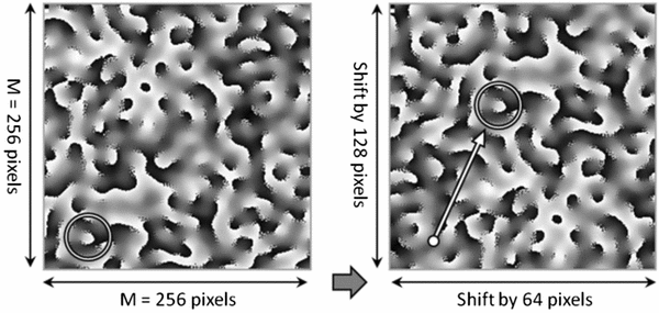
Periodic kinoform shift demonstrated on a 256 × 256 pixel CGH. The periodic shift is 64 pixels. The CGH is shifted once (64 pixels) along the horizontal axis and twice (128 pixels) along the vertical axis. The circle tracks a single feature being shifted
-
(c)
Our novel laser marking approach, as shown conceptually in Fig. 4. In this case, a CGH combined with the FZL is used to generate an array of diffractive beams (beamlets). The beamlets are used to mark in parallel small areas (subpixels) of the checkerboard squares. The top left (first) subpixels of all squares are illuminated for the first frame of the SLM (13.33 ms). The whole kinoform (CGH + FZL) is then shifted prior to the second frame in order to translate the array of beamlets by one subpixel to the right, and afterwards mark the second subpixel of each checkerboard square. This process is continued until all 16 subpixels have been marked. The translation of the beamlet array across the processing plane is possible by means of the FZL, which is moved off-axis using the Holoeye software.
Fig. 4 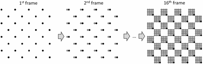
The concept of the novel laser marking method described in (c) below. Black and gray dots represent currently and post-marked subpixels of the checkerboard, respectively
-
(d)
An alternative approach to (c) in which 16 different CGHs are used to sequentially mark the checkerboard pattern. Again, the checkerboard squares are marked in parallel, using 16 successive frames—each of which generates an array of subpixels. However, rather than moving the whole kinoform (CGH + FZL) between each frame (laser irradiation), a different CGH design (together with on-axis FZL) is instead used to generate each of the subpixel arrays.


4 Experimental results
Figure 5 shows the checkerboard patterns which were produced by using one of the four laser-marking approaches described in “Experimental protocol”—in the same order. Patterns presented in Fig. 5(a) and (b) were generated at an average laser power of P = 7.1 W, using 16 × 13.33 ms trains of laser pulses. The laser marked areas of Fig. 5(a) and (b) clearly suffer from speckle interference, even though the pattern in Fig. 5(b) was marked using the time-averaging technique, as described in (b). Although this technique can efficiently reduce speckles, as reported in [8], in our case, the reduction was inefficient because the marked areas were significantly smaller.

Checkerboard pattern produced using four different approaches: a basic approach, b time-averaging technique, c our new laser-marking approach, and d an alternative approach to c. Patterns (a) and (b) were generated at P = 7.1 W, while patterns (c) and (d) were produced at P = 2.25 W
The checkerboard in Fig. 5(c), meanwhile, which shows no evidence of speckle, was obtained using our new approach [described in (c)]. The average laser power used for marking the pattern was approximately three times lower (P = 2.25 W) than for approaches (a) and (b), whilst the other laser machining parameters were unchanged. To generate the checkerboard, the whole kinoform (CGH + FZL) was repeatedly moved off-axis with a step of seven pixels (as defined in the Holoeye software) prior to each train of laser pulses. The marked subpixels of the checkerboard were measured to be approximately 7 μm in diameter. Since the subpixels were exactly adjacent for the kinoform shift of 7 pixels, it is clear that the experimental setup provided a positional accuracy of less than 1 μm. Here, it should also be mentioned that we were not able to mark the checkerboard pattern at the laser power of 2.25 W when approaches (a) and (b) were applied. This is because in these approaches the amount of the output laser power was redistributed over a larger area of the diffractive pattern (i.e., the whole checkerboard pattern), rather than being focused in only 16 beamlets, reducing the effective optical intensity required to ablate the workpiece. The use of a lower laser power for marking is a major advantage of approaches (c) and (d), because the average laser power handling capabilities of commercially available SLMs do not exceed typically 2-3 W/cm2 unless an additional cooling system is applied.
Although a similar quality checkerboard pattern can be obtained using the alternative laser marking approach [i.e., approach (d)], as can be seen in Fig. 5(d), this method does not provide such precise movement of the array of subpixels because the movement is limited to only one sub-pixel in terms of the target image design. If we consider the experimental setup shown in Fig. 1, this corresponds to a 7 μm shift at the workpiece surface, while our preferred approach [i.e., approach (c)] allows the array of beamlets to be shifted with a step of approximately 1 μm, and hence it provides higher resolution marking. To obtain such a precise movement of the workpiece under the highly-focused laser beam, it would be necessary to use high-accuracy translation stages, but this approach could significantly increase the laser marking time due to the entirely sequential (point-by-point) laser marking approach. The benefit of adopting a different CGH design in approach (d) is that each CGH is optimized for each individual image generated by the SLM, and therefore the distribution of speckles is naturally random. However, in our case, i.e., when a CGH generates an array of subpixels, the speckles are not the serious problem, because a separation distance between the individual subpixels is large enough to avoid interference between beamlets. As shown in Fig. 5, there is no need to design 16 different CGHs and load them onto the SLM individually for each laser pulse train—like in approach (d)—to provide high quality ablation. Therefore, the laser marking time in approach (c) is in fact less than that in approach (d) because only one CGH is loaded onto the SLM and used for the whole marking process.
The defocused zero-order beam can cause serious surface damage to the sample if the intensity of the zero-order beam at the processing plane is greater than the ablation threshold of the substrate [11]. To avoid such damage, the separation distance between the planes of the focused zero-order beam and the diffractive pattern must be carefully selected. Then, the diffracted multiple beams will ablate the substrate in the desired areas whilst the defocused zero-order beam will not cause any damage to the surface. The separation distance for which the sample is not damaged by the defocused zero-order beam depends on the focal length of the final focusing lens used in the optical setup. If a relatively short focal length is used, e.g., the 30 mm FL lens used in our experiments, the separation distance can be 1.5 mm (or even less). If a relatively long focal length lens is used, e.g., the 100 mm F-theta lens used in the experiments described in [11], the separation distance must be at least 5 mm.
5 Generation of complex micropatterns using our laser marking approach
Many manufacturers are obliged to mark their products and components to provide necessary information about the goods to suppliers and customers. Marks are used for primary identification (e.g., company name, part number), traceability (e.g., serial number), compliance control of products (e.g., CE mark), and for anti-counterfeiting. Marks can contain alphanumeric characters, symbols, trademarks, and also data-coded information in the form of barcodes, QR codes, or datamatrices. When the product is relatively large, the marking process is quite straightforward. However, if the product is very small (less than a couple of millimeters) it is very difficult to generate a mark that will contain necessary information about the product. Therefore, there is a need to provide a technique for marking, which will allow marks to be located on a very small scale.
In this section, we present a possible application of our laser-marking approach for secure data coding of small metal parts. Figure 6 shows a 20 × 20 datamatrix containing coded information of 22 alphanumeric characters. This code, when is magnified, is readable using, e.g., a smartphone with a downloaded datamatrix reader. Since the datamatrix design was larger than the checkerboard pattern shown in Fig. 5 and was constructed using 223 beamlets from the CGH, it proved necessary to increase the output laser power to 10.9 W in order to achieve ablation of the metal. As before, we used 16 laser irradiations (16 × 13.33 ms trains of laser pulses), but this time the FZL was set up to give an approximately 1 mm separation distance between the planes of the focused zero-order beam and the diffractive pattern. This approach not only allowed the datamatrix (square) pixels to be reduced in size to only 15.5 μm, but also reduced the size of the defocused zero-order beam at the processing plane (and hence increased the ‘background’ intensity that this zero-order provides), and thus decreasing the minimum laser power required to ablate the substrate. However, because the separation distance between the individual beamlets was shorter than that used for generating the checkerboard pattern (see “Experimental results”), the 20 × 20 pixel datamatrix suffered from small-scale speckles, as can be seen in Fig. 6(b), due to mutual interference of the neighbouring beamlets. Moreover, it can be observed in Fig. 6 that the edges of the datamatrix are slightly faded in comparison to the centre. This results from the fact that the IFTA used in our experiments did not optimize a CGH in terms of the intensity uniformity of the diffractive image generated by the CGH. More uniform intensity distribution within the diffractive image, however, could be obtained by: (a) designing a CGH for the actual shape of the laser beam delivered to the SLM display, (b) using a feedback closed-loop control for optimising the CGH [14, 15], or (c) using different algorithms for generating a CGH [16, 17]. Another reason for the fading can be aberrations generated by the optical system because the effective focal length of the setup was decreased in order to obtain a datamatrix of less than 320 μm by 320 μm.

a Datamatrix containing a code with 22 alphanumeric characters. This datamatrix was produced on the surface of Chromflex steel using our invented laser-marking method at P = 10.9 W. b Close-up view of the left-bottom corner of the datamatrix shown in a
The time required for the generation of the datamatrix shown in Fig. 6 has been estimated to be approximately 0.6 s (16 × 13.33 ms for laser marking and approximately 0.4 s for shifting the whole kinoform between the subsequent laser irradiations). This means that 100 similar micropatterns can be produced within one minute. Although the processing time seems to be acceptable for mass-marking, such small datamatrices could be produced in an even shorter time if an SLM with higher frame rate was available. Recently, we have found that high quality markings can be generated even with 400 pulses/pixel (compared with the 5333 pulses/frame used here), providing the opportunity to reduce the laser marking time of 20 × 20 pixel datamatrices to less than 0.42 s.
Another solution for reducing the fabrication time of the datamatrices is to introduce a galvo-scanner or polygon scanner to the laser marking setup. This approach, however, does not allow (with a standard F-theta lens) the features to be marked with dimensions as small as those obtained by the SLM—using either approach (c) or (d). Moreover, galvo-scanners provide a laser beam positioning error, which can be greater than 2 μm, and of course, they use moving parts (mirrors) which can be a problem when the galvo scanning system is exposed to external vibrations, e.g., when used for marking products in mass production.
Finally, we report that we used our laser marking approach to generate a number of different micropatterns (not shown in this paper). All of them had very good mark quality without visible speckles. This indicates that our laser marking approach is reliable and potentially can be transferred to industry for marking small components.
6 Conclusion
We have experimentally demonstrated a simple but novel SLM-based laser marking approach in which an array of beamlets is used for parallel marking the array of subpixels to build-up arrays of square pixels. This approach allows complex micropatterns to be produced on the workpiece without visible speckles. This means that such patterns can be easily read with an optical microscope equipped with the datamatrix reader. We believe that this new marking approach will find application in medicine, industry, and military for secure data coding of small and valuable parts, such as stents, microchips, car/aeroengine components, etc.
Although it is possible to generate small micropatterns by entirely sequential marking using a galvo scan-head with a single focused laser beam, datamatrices with such small-scale square pixels would be difficult to achieve with standard galvo scanning systems. Our new SLM-based sequential–parallel approach, meanwhile, provides an efficient and throughput, high precision process without the need for moving parts, which can be beneficial when the marking process must be performed in the environment that is exposed to external vibrations (e.g., in line production).
In this paper, sequential–parallel processing using diffractive multiple beams generated by an SLM has been demonstrated for producing speckle-free micropatterns. Although this work was focused on marking of metal surfaces, the same approach can also be used for processing other materials, such as glass, semiconductors and polymers. We believe that our technique, when additionally combined with translation stages for moving the substrate, can be exploited in many other applications, e.g., high throughput pattering/structuring of surfaces or direct laser writing of 3D optical components/devices.
References
Y. Hayasaki, T. Sugimoto, A. Takita, N. Nishida, Appl. Phys. Lett. 87, 031101 (2005)
D. Liu, Z. Kuang, W. Perrie, P.J. Scully, A. Baum, S.P. Edwardson, E. Fearon, G. Dearden, K.G. Watkins, Appl. Phys. B 101, 817–823 (2010)
R.J. Beck, J.P. Parry, W.N. MacPherson, P.D. Hand, Opt. Express 18, 17059–17065 (2010)
Z. Kuang, W. Perrie, D. Liu, P. Fitzsimons, S.P. Edwardson, E. Fearon, G. Dearden, K.G. Watkins, Appl. Surf. Sci. 258, 7601–7606 (2012)
Y. Hayasaki, M. Nishitani, H. Takahashi, H. Yamamoto, A. Takiita, D. Suzuki, S. Hasegawa, Appl. Phys. A 107, 357–362 (2012)
Z. Kuang, W. Perrie, J. Leach, M. Sharp, S.P. Edwardson, M. Padgett, G. Dearden, K.G. Watkins, Appl. Surf. Sci. 255, 2284–2289 (2008)
L. Golan, S. Shoham, Opt. Express 17, 1330–1339 (2009)
J.P. Parry, R.J. Beck, J.D. Shephard, D.P. Hand, Appl. Opt. 50, 1779–1785 (2011)
B. Redding, M.A. Choma, H. Cao, Nature Photon. 6, 355–359 (2012)
J.A. Davis, A.M. Field, D.M. Cottrell, Appl. Opt. 34, 790–792 (2009)
Z. Kuang, W. Perrie, D. Liu, S.P. Edwardson, J. Cheng, G. Dearden, K.G. Watkins, Appl. Surf. Sci. 255, 9040–9044 (2009)
F. Wyrowski, O. Bryngdahl, J. Opt. Soc. Am. A: 5, 1058–1065 (1988)
R.J. Beck, J.P. Parry, J.D. Shephard, D.P. Hand, Appl. Opt. 50, 2899–2905 (2011)
J.S. Liu, M.R. Taghizadeh, Opt. Lett. 27, 1463–1465 (2002)
J.S. Liu, M. Thomson, A.J. Waddie, M.R. Taghizadeh, Opt. Eng. 43, 2541–2548 (2004)
R. Di Leonardo, F. Ianni, G. Ruocco, Opt. Express 15, 1913–1922 (2006)
S. Hasegawa, Y. Hayasaki, Opt. Lett. 36, 2943–2945 (2011)
Acknowledgments
The research covered in this paper was funded by the Engineering and Physical Sciences Research Council (EPSRC), Heriot-Watt Innovative Manufacturing Research Centre (HW-IMRC, Grant No.: EP/F02553X/1), the Finnish Funding Agency for Technology and Innovation (TEKES), and our industrial partner Renishaw Plc. (UK).
Author information
Authors and Affiliations
Corresponding author
Rights and permissions
Open Access This article is distributed under the terms of the Creative Commons Attribution License which permits any use, distribution, and reproduction in any medium, provided the original author(s) and the source are credited.
About this article
Cite this article
Wlodarczyk, K.L., Kaakkunen, J.J.J., Vahimaa, P. et al. Efficient speckle-free laser marking using a spatial light modulator. Appl. Phys. A 116, 111–118 (2014). https://doi.org/10.1007/s00339-013-8186-1
Received:
Accepted:
Published:
Issue Date:
DOI: https://doi.org/10.1007/s00339-013-8186-1