
Abstract
The solid state particle detectors emerged in 1950. Initially Si and Ge detectors operated as junction diodes were used for charged particle detection and γ spectroscopy measurements. Although these detectors are superior to gaseous detectors in many respects, being a crystalline medium meant that they are susceptible to radiation damage. Unlike in gaseous detectors where the detection media can be exchanged the semiconductor crystals have to retain their detection properties over the entire envisaged period of operation. The particle detection capabilities and the energy resolution degrade gradually with irradiation, which limits their lifetime.
You have full access to this open access chapter, Download chapter PDF
21.1 Introduction
The solid state particle detectors emerged in 1950 [1]. Initially Si and Ge detectors operated as junction diodes were used for charged particle detection and γ spectroscopy measurements (Chap. 5). Although these detectors are superior to gaseous detectors in many respects, being a crystalline medium meant that they are susceptible to radiation damage. Unlike in gaseous detectors where the detection media can be exchanged the semiconductor crystals have to retain their detection properties over the entire envisaged period of operation. The particle detection capabilities and the energy resolution degrade gradually with irradiation, which limits their lifetime.
A large majority of present high energy experiments uses position sensitive silicon detectors which became widely available after the introduction of planar process in 1980 [2]. Their goal is achieving desired position resolution with as few read out channels as possible, while keeping detection efficiency close to 100%. At the present and particularly future experiments high particle rates close to the interaction point require very fine segmentation and high position resolution of detectors in order to be able to associate hits with tracks.
In the future a precise timing information associated with a track and even with each sensor hit may be required to cope with large multiplicity of tracks. The sensor hits and associated tracks will be therefore separated not only spatially, but also in time allowing easier assignation of tracks to different collisions occurring within each colliding particles bunch crossing.
High particle rates cause radiation effects. The most important is the damage of the crystal lattice which leads to the degradation of the measured charge after passage of ionizing radiation. At the same time the noise may increase for various reasons thus significantly reducing the signal-to-noise ratio. Consequently the detection efficiency, energy, and position resolution may degrade to the level where the detectors become unusable. Extensive research was made in the last decades to understand the damage in silicon detectors and to manipulate the properties of silicon aiming at radiation-harder detectors. The research was not only limited to silicon but alternative semiconductor materials were considered.
It is not only the bulk crystal that is affected by irradiation, but also the surface. The radiation effects at the silicon—silicon oxide interface not only change the performance of silicon detectors, but are the main reason for radiation damage of electronics. The latter was often considered a bigger problem than the radiation damage of detectors, particularly in environments where the ionization dose was large (e.g. synchrotron radiation). With the advent of deep sub-micron CMOS processes, electronics was thought to became intrinsically radiation hard and no special radiation hardening processes would be required. An important contribution to the radiation hard electronics was also introduction of radiation-tolerate design rules. However, for very small feature sizes, e.g. very deep sub-micron processes, such as 0.130, 0.065 μm, radiation hardness of electronics, rather than sensors, could become a limiting factor at harshest radiation environments.
On the other hand the effects of radiation damage were exploited for dose measurements. Active dosimeters appeared for both measurements of ionizing and non-ionizing energy losses in silicon crystal such as p − i − n diodes [3] and radiation sensitive field effect transistors [4].
21.2 High Radiation Environments
The radiation environments differ in composition and energies of the particles producing the radiation damage. Although the particles that are to be detected contribute largely to the damage it is often the background particles that dominate. As will be described later the damage depends on the type of the particle. While X-rays alter the properties of the detector surface they can not displace the semiconductor atoms from the lattice. On the other hand neutron irradiation affects only the lattice and energetic charged hadrons and leptons damage both the lattice and the surface. The difference in damage creation and its effects to detector operation will be discussed later. First we review the radiation environments where particle detectors are employed.
Collider Experiments
In general there are three major types of accelerators with respect to collision particles: hadron (p − p, \(\bar {p}-p\), heavy ions), lepton (e + − e −, eventually μ+ −μ−) and lepton-hadron (e +, −− p). The flux of particles traversing the detectors is given by the particles originating from the collisions (ϕ coll) and secondary radiation that originates from the spectrometer or the accelerator (ϕ sec)
The flux of particles crossing the detectors is much larger at hadron colliders than at lepton colliders, owing to a difference in total cross-section σ tot of colliding particles. The radiation environment at lepton colliders is dominated by e± from Bhaba scattering. Consequently the radiation damage of detectors at hadron colliders is much more severe than at lepton colliders.
A significant secondary irradiation, particularly at high luminosity colliders, can arise from back-scattered neutrons originating in breakup of nuclei in calorimeters and other parts of spectrometers after interaction with highly energetic hadrons. The secondary radiation originating from the accelerator such as synchrotron radiation, beam-gas interactions or halo particles scraping the collimators should be small but can represent in case of an accident a significant contribution to the total fluence Φ (integral of flux \(\Phi =\int \phi \,dt\)) of particles traversing the detectors.
The required radiation tolerance/hardness of vertex detectors at different colliders is given in the Table 21.1. Placing of the detectors in the spectrometer determines their exposure. The ϕ coll decreases quadratically with the distance from the interaction point. The large cross-section for soft collisions result in larger ϕ coll at small angles with respect to beam. Large ϕ coll at small angles is also characteristic for asymmetrical beams (energy, particle) or fixed target experiments. A particle fluence profile for ATLAS experiment [5] at the Large Hadron Collider (LHC) is shown in Fig. 21.1. The dominating particles are at small radii mainly pions and protons originating from collisions and “albedo” neutrons from the calorimeters for R > 20 cm.

Yearly fluence profile in ATLAS experiment at LHC design luminosity. The radiation damage caused by different particles was used to normalize the fluences (see next section for Φeq). The arrows denote the location of the pixel and strip detectors (SCT)
The choice of detector technology at a given radius depends on the ability to retain the detection efficiency and position resolution at required levels. At the same time the material budget should be kept low in order not to spoil the tracking performance. At many experiments the most exposed detectors are beam position/condition and radiation monitors (Chap. 18).
Space Applications
Particle detectors are an important constituent of many space missions. They are mainly used as spectrometers, visible light detectors and charged particle trackers. The radiation fields are far less severe than that at accelerators experiments, but the detectors and the information that they provide can be far more susceptible to the radiation effects (e.g. CCD, DEPFet, Si-drift detectors). The origin of radiation in space comes from three sources:
-
Galactic cosmic radiation; Consists primarily of nuclei (85% protons, 14% Helium, 1% heavier ions among which Fe and C are most abundant ones). The relevant particles for damage creation have energies between 1–20 GeV. The fluxes of cosmic particles are shown in Fig 21.2a. The flux depends on the activity of the sun through interaction with solar wind (a continuous stream of high ionized plasma emerging from the sun). Interactions of highly energetic particles with nuclei in the earth’s atmosphere or space-vessel produce showers of ionizing particles which increase the intensity of the radiation.
-
Solar particles; The sun is also a sporadic source of lower energy charged particles (solar particles) accelerated during certain solar flares and/or in the subsequent coronal mass ejections. These solar particles comprise both protons and heavier ions with variable composition from event to event. Energies typically range up to several hundred MeV and occasional events produce particles of several GeV. Although such events are rare, typically one per month and lasting several hours to days, the flux integrals as large as 1010 cm−2 for protons with energy >1 MeV were measured.
-
Radiation belts; The charged particles trapped in the Earth’s magnetic field form so called Van Allen’s belts. The inner belt extends to 2.5 Earth radii and comprises protons up to 600 MeV and electrons up to several MeV. The outer belt extends to 10 Earth radii where there are mainly electrons and soft protons (0.1–100 MeV). The fluxes of electrons and protons trapped in the radiation belts are shown in Fig. 21.2b. The sharp fall of flux at high energies makes shielding very effective.

Environmental Applications
-
Medical application; The most widely used source of radiation are X-rays, Linacs and radio active isotopes used for cancer treatment. The energy of photons used is: up to 100 keV for X-rays, below 1 MeV for isotopes and up to 25 MeV for Linacs.
-
Fusion in fission reactors and nuclear waste managements; The main damage comes from neutrons and γ rays, both with energies up to few MeV. Fusion reactors of TOKAMAK type require plasma, fuel impurity and fusion products monitoring instrumentation close to the first wall. The foreseen neutron fluences to which the sensors (e.g. silicon sensors for X-ray spectroscopy) and electronics will be exposed at International Thermonuclear Experimental Reactor (ITER) are comparable with that of the HL-LHC, up to few 1016 cm−2.
21.3 Damage Mechanism in Solid State Detectors and Electronics
As radiation (photons, leptons, hadrons) passes through material, it loses energy by interaction with the electrons and nuclei of the material atoms. The effects produced in the material are dependent on the energy-loss processes and the details of the material structure. The damage in semiconductor detectors can be divided into bulk and surface damage.
21.3.1 Bulk Damage
The interaction with electrons results in creation of electron-hole pairs (ionizing energy loss, ionizing dose) that does not affect the lattice and causes no bulk damage. The bulk damage in crystalline and poly-crystalline material is a consequence of displacement of lattice atoms by impinging particles, due to elastic scattering on a nuclei and nuclear reactions. In order to produce Primary Knocked off Atom (PKA) the transfer of kinetic energy should be sufficient. Approximately 25 eV of recoil energy is required for example in silicon. The displaced atom may come to rest in a interstitial position (I), leaving a vacancy (V) at its original location. If the kinetic energy of the recoiling atom is sufficient (∼5 keV in Si [8]) it can displace further atoms, creating a dense agglomeration of defects at the end of the primary PKA track. Such disordered regions are referred to as defect clusters.
Most of the resulting vacancies and interstitials recombine while others diffuse away and eventually create stable defects with impurity atoms and other vacancies or interstitials. Those defects disturb the lattice periodicity and give rise to energy levels in the band-gap, which alter the properties of the semiconductor. In most semiconductor materials the cross-section for nuclear reaction is much smaller than for elastic scattering, hence the creation rate of defects, resulting from nuclear reactions, is usually more than two orders of magnitude lower when compared to creation rates of defects originating from displaced silicon atoms.
The energy E p required for an incoming particle of mass m p to produce PKAs and clusters with a creation threshold E th can be calculated from non-relativistic collision kinematics as
where the lattice atom has a mass m l. In silicon a neutron needs at least 175 eV to produce a PKA and 35 keV to form a cluster. For an electron a relativistic kinematics should be used giving 260 keV and 8 MeV. It should be noted that the radiation damage caused by γ-rays from radioactive decays is primarily due to the interaction of Compton electrons with a maximum energy well below the one required for cluster production. The bulk damage is therefore exclusively due to point defects. As the thresholds are of the same order also in other semiconductor materials (see Table 21.2 ) similar conclusions are valid.
A part of vacancies and interstitials formed immediately after irradiation can recombine, while others diffuse away and eventually recombine or react with other defects or impurities. The defects can evolve in time. They can either dissociate or react with each other and form new defects. The evolution of defects is described by first order dynamics in case of dissociation (Eq. (21.3)) or second order dynamics for reactions of two defects (Eq. (21.4)):
where \(k_{1,2}^Y\) denotes the reaction constants. The Eq. (21.4) turns into a first order process in cases when one type of the reacting defects is present in much larger quantities than the other. The solution of Eq. (21.3) is exponential with
with \(N^0_{X}\) denoting the initial concentration of defects X proportional to the fluence. The solution of the Eq. (21.4) for (\(N^0_{X_A} > N^0_{X_B}\)) is given by
In the case of two defects with similar initial concentrations \(N^0_{X_A} = N^0_{X_B}= N^0_{X}\) or a reaction between defects of the same type one obtains
From Eqs. (21.3) and (21.4) it can be seen that for first order reactions, the rate depends linearly on defect concentration while for second order reactions the dependence is quadratic.
Since the energy needed for breaking up the defect (dissociation) or forming a new defect is supplied by the lattice vibrations, the reaction constant is strongly temperature dependent. The lattice atom vibration energy is governed by the Maxwell-Boltzmann distribution. The probability of sufficient energy transfer from lattice vibration to the defect is therefore exponential with temperature (T). If the reaction rate given by the Arrhenius relation is known at T 0 then the rate at T 1 is calculated as:
where E a is the energy required for defect dissociation or formation.
21.3.1.1 Non-Ionizing-Energy-Loss Hypothesis of Damage Effects
The energy loss of impinging particles suffered in a process of displacing lattice atoms is called non-ionizing energy loss—NIEL. First experimental findings have led to the assumption that damage effects produced in the semiconductor bulk by energetic particles may be described as being proportional to non-ionizing energy loss, which is referred to as the NIEL-scaling hypothesis. According to it any displacement damage induced change in the material properties scales with the amount of energy imparted in displacing collisions, irrespective of the spatial distribution of the defects in a PKA cascade and irrespective of the various annealing sequences taking place after the initial damage [10].
The non-ionizing energy deposit in a unit cell of the target nuclei (ρ dis) exposed to the fluence of particles with energy E can be calculated as
where D(E) [9] is so-called displacement damage function, sometimes also referred to as damage cross-section. For a spectrum of particles the contributions to the ρ dis for each energy should be summed:
According to NIEL hypothesis ρ dis determines the damage effects. The damage efficiency of any particle spectrum d Φ∕dE can therefore be expressed as that of an equivalent 1 MeV neutron fluence. The equivalent fluence of 1 MeV neutrons Φeq is calculated as
where κ is so called hardness factor for that particle spectrum and D n(1 MeV) the D for 1 MeV neutrons, 95 MeV mb for Si and 10 MeV mb for diamond [12]. The displacement damage cross-section for pions, protons, electrons and neutrons in silicon is shown in Fig. 21.3. The hardness factors for most commonly used irradiation facilities are given in the Table 21.3.

Non Ionizing Energy Loss NIEL for different particles in silicon [11]. The insert shows magnified D(E) for most damaging particles at LHC
The NIEL hypothesis is violated in silicon for highly energetic charged hadrons. In addition to the hard core nuclear interactions, being dominant for neutrons, charged hadron reactions are also subjected to Coulomb interactions leading to low energy recoils below the threshold for cluster creation. In this case the damage is a mixture of homogeneously distributed point defects and clusters. This distinct difference between neutron and proton induced damage is depicted in Fig. 21.4. Different impurities (e.g. O,C) are homogeneously distributed over the volume and the probability for such an impurity to form a defect complex with vacancy or interstitial is much larger if the latter are also homogeneously distributed. Hence, the defects formed after irradiation and consequently the lattice properties can be different for various irradiation particles at equal NIEL. It should be emphasized again that the NIEL scaling can only be regarded as a rough approximation as it disregards the specific effects resulting from the energy distribution of the respective recoils.

Initial distribution of vacancies produced by 10 MeV protons (left), 23 GeV protons (middle) and 1 MeV neutrons (right). The plots are projections over 1 μm of depth (z) and correspond to a fluence of 1014 cm−2 [10]
21.3.1.2 Impact on Bulk Damage on Detector Performance
As already mentioned the defects in the semiconductor lattice give rise to energy levels (states) in the band gap affecting the operation of semiconductor detector mainly in three ways as shown in Fig. 21.5.
-
Some of the defects can be charged which leads to (Chap. 5) (Fig. 21.5a) changes in the electric field. For semiconductor detectors this may result in loss of the depleted (active) region requiring an increase of the applied bias. The bias voltage is however limited by the device break down. The space charge is calculated as a difference in concentration of charged donors and charged acceptors,
$$\displaystyle \begin{aligned} N_{eff}\, =\,\sum_{donors} N_t\,(1-P_t)\,-\,\sum_{acceptors} N_t\,P_t , {} \end{aligned} $$(21.14)where N t denotes the concentration of deep traps and P t the probability of a trap being occupied by an electron. The traps continuously emit and capture carriers. The difference in emission and capture rate is called the excess rate. In a stationary state the occupation probability is constant, therefore excess rates of holes and electrons for a given trap have to be equal. The derivation of occupation probability from this condition can be found in any solid state physics text book. As the P t is needed for calculation of detector properties we will just state the result:
$$\displaystyle \begin{aligned} P_t\,& = \,\biggl[\frac{c_p\,p\,+\,\epsilon_n}{c_n\,n\,+\,\epsilon_p}+\,1 \biggr]^{-1} , {} \end{aligned} $$(21.15)$$\displaystyle \begin{aligned} c_{n,p} & = \,v_{th_{e,h}}\,\sigma_{t_{e,h}} , \epsilon_{n,p}=n_i \, c_{n,p}\, \mathrm{exp}(\pm\frac{E_t-E_i}{k_B\,T}) . {} \end{aligned} $$(21.16)where c n,p is the capture coefficient and 𝜖 n,p emission rate of electrons and holes, respectively. The concentration of free electrons and holes is denoted by n and p and their thermal velocity by \(v_{th_{e,h}}\). The capture coefficients and emission rates depend on trap and semiconductor properties. The carrier capture cross-section is given by \(\sigma _{t_{e,h}}\) and the level in the band gap by E t. The Fermi level and free carrier concentration in intrinsic semiconductor are denoted by E i and n i. They occupation probability depends on temperature only for levels close to middle of the band-gap. The exponential term in Eq. (21.15) prevails once E t is few k BT away from the E i. If follows from here that only donors in the upper part of the band gap and acceptors in lower part of the band gap contribute to the space charge.
Fig. 21.5 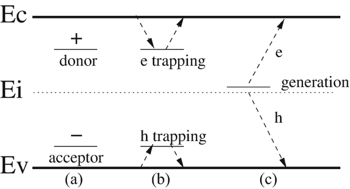
Consequences of deep energy levels to operation of semiconductor detectors: (a) charged defects alter the space charge and therefore the electric field, (b) defects can trap and detrap free carriers and (c) defects act as generation-recombination centers. Electrons and holes are denoted by e and h
-
The states can act as trapping centers for the drifting charge generated by the particles we want to detect (Fig. 21.5b). If trapped charges remain trapped and do not complete the drift within the integration time of the read-out electronics they are lost for the measurement, which leads to smaller signal.
The probability for electrons and holes to be trapped at the trap t can be calculated as
$$\displaystyle \begin{aligned} \frac{1}{\tau_{{tr}_{e}}^t}\,=\,c_n \,(1\,-\,P_t)\,N_t , \quad \frac{1}{\tau_{{tr}_{h}}^t}\,=\,c_p \,P_t\,N_t . {} \end{aligned} $$(21.17)The trapping time \(\tau _{{tr}_{e,h}}^t\) represents the mean time that a free carrier spends in the part of the detector before being trapped by t. According to Eq. (21.17) electron traps have energy levels in the upper part of the band gap (P t ≈ 0), while hole traps have energy levels in the lower part of the band gap (P t ≈ 1).
To get the effective trapping probability \(1/\tau _{{eff}_{e,h}}\) for electrons and holes one has to sum over the trapping probabilities of all traps with emission times (1∕𝜖 n,p) longer than integration time of the electronics:
$$\displaystyle \begin{aligned} \frac{1}{\tau_{{eff}_{e}}}\, & =\,\sum_{t}^{defects} \ c_{n} \, (1-P_t)\, N_t , \end{aligned} $$(21.18)$$\displaystyle \begin{aligned} \frac{1}{\tau_{{eff}_{h}}}\, & =\,\sum_{t}^{defects} \, c_{p} \, P_t\, N_t . {} \end{aligned} $$(21.19)The emission times decrease with distance from the mid-gap and become at certain energy level short enough not to be included in the Eq. (21.19). The traps close to the mid-gap have therefore a dominant contribution to the effective trapping times.
-
States close to the mid-gap region also act as generation-recombination centers (Fig. 21.5c). The thermally generated electron hole pairs are separated in the electric field before they can recombine, which gives rise to the bulk generation current. The increase of current leads to the increase of noise and power dissipation.
The generation current can be calculated with the assumption of equal generation rates G t = G n = G p of electrons and holes in thermal equilibrium:
$$\displaystyle \begin{aligned} G_t\,&=\,N_t\,P_t\,\epsilon_n = N_t \, \frac{\epsilon_n\,(\epsilon_p + c_n\,n)}{\epsilon_n+\epsilon_p+c_p\,p+c_n\,n} \end{aligned} $$(21.20)$$\displaystyle \begin{aligned} G_t\,&=\,N_t\,\frac{1}{1/\epsilon_n+1/\epsilon_p} \quad \mathrm{for} \quad n,p\approx 0 . {} \end{aligned} $$(21.21)Both carrier types generated in the active volume drift to the opposite electrodes. The current density, albeit different for holes and electrons, is constant everywhere in the detector. The measured current is therefore calculated as
$$\displaystyle \begin{aligned} I\,=\,e_0\,w\,S\,\sum_{t}^{defects} G_t {} \end{aligned} $$(21.22)where w denotes the active thickness and S the active surface of the detector. It follows from Eq. (21.21) that only the levels close to mid-gap E i ∼ E t contribute significantly to the current. If traps are far from the mid-gap, emission times are either very long or very short.

Apart from the changes in the depletion region, the properties of the non-depleted silicon bulk are also affected by irradiation. The resistivity of the bulk increases. The increase depends on both initial dopant concentration as well as on irradiation fluence. The minority carrier lifetime also decreases as 1∕τ r ∝ Φ and reaches values of few tens ns at Φ = 1014 cm−2 and below ns at Φ > 1016 cm−2 [13].
Recent measurements [14] also show that mobility of free carriers is affected by radiation. The concentration of defects, not only electrically active, is high enough to affect the low field mobility. A significant decrease of low field mobility was observed at fluences of Φeq > 5 ⋅ 1015 cm−2.
Although silicon detectors are by far the most widely used there are other semiconductor detectors which can be used in high radiation fields and have a higher PKA displacement energy. The material properties of different semiconductors used as particle detectors are summarized in Table 21.2.
Effects of irradiation on detector performance strongly depend on the choice of material. In wide band gap semiconductors for example the rate of thermally generated carriers will be small even if states close to mid-gap are present in abundant concentrations due to small intrinsic carrier concentration. Thus the leakage current increase is negligible. If the drift velocity is large and charge collection time is short then the increase of trapping probability will be less important. The small dielectric constant reduces the capacitance of a detector leading to lower noise, which can partially compensate for larger e-h pair creation energy. The choice of the semiconductor detector for a specific application is often governed by a compromise in semiconductor properties. Also availability, reliability and experience play an important role. In this respect diamond is the choice of detector material next to silicon.
21.3.1.3 Most Important Defects in Silicon
A lot of effort was invested over the R&D phases of LHC/HL-LHC in identifying the defects responsible for changes in performance of silicon detectors. A comprehensive list of defects identified by so called “microscopic” techniques such as Deep Level Transient Spectroscopy (DLTS) or Thermally Stimulated Current (TSC) can be found in [15]. The summary plot with the most important defects is shown in Fig. 21.6. The effects for which they are mainly responsible will be addressed in the following sections. Note, that for only few identified energy levels the chemical composition of the corresponding defects is known.

A schematic view of known defects and their main effects on the detector performance. The defect charge state is given in brackets. For the defects with unknown chemical composition the temperature at which electron -E or hole-H traps were identified with DLTS/TSC techniques is used. The near mid-gap H levels are likely multivacancy complexes
21.3.2 Surface Damage
The semiconductor detector bulk needs to form a contact with readout electronics. The contacts used, either Ohmic or Schottky, as well as the rest of the surface are prone to changes due to irradiation. The description of surface radiation damage given here will be focused on the border of silicon bulk and oxide (Chap. 5). The surface damage affects the electrical properties of the detectors such as inter-electrode resistance, inter-electrode capacitance and dark current. It is particularly important for sensors where charge flow is close to the surface, such as 3D-Si detectors, CCDs, Active CMOS Pixel Detectors and MOS-FET transistors.
The surface of particle detectors is usually passivated by thermal oxidation [16]. The oxide isolates and stabilizes the crystal surface with respect to chemical and electrical reactivity. The cross-section of the device surface is generally divided into silicon/oxide interface and oxide bulk depicted in Fig. 21.7. The border region between oxide and silicon crystal is characterized by a large defect density due to bond stress. In general surface defects can be caused by growth and irradiation. According to their position in the oxide the traps are divided in the oxide bulk traps (OT), border traps (BT) and interface traps (IT). The latter two are located close to the interface and can exchange charges with underlying silicon (switching traps). The oxide traps are mostly donors, which is the reason that net oxide charge density is always positive. The most important oxide defects are trivalent Si (≡ Si⋅, donor), interstitial oxygen (OI, donor) and non-bridging oxygen (≡ Si–O⋅, acceptor). Other important defects include hydrogen related defects (all donors) [18]. Hydrogen is particularly important since it passivates the dangling bonds by attaching to them. The build-up of interface traps is not fully understand yet and there are different models explaining it [18, 19]. The bulk and interface traps formed during processing of the oxide can be passivated by annealing (350–500∘C) in hydrogen rich environment.

Schematic view of the surface of a silicon detector according to [17]; (a) surface regions (b) trap locations (c) states (d) oxide charges
If the creation of e–h pair in the silicon bulk is completely reversible process, it is not in SiO2 and at the interface. Ionizing radiation has a significant impact on the defect generation and activation. The damage mainly manifests itself as a regeneration process of already present but deactivated defects. Hence the processing of the oxide, preparation and temperature treatments (annealing) impacts the performance after irradiation.
Although the underlying physics of formation is not yet fully understood, it is assumed that radiation ionizes oxide bulk defects that remain charged
or free holes are trapped by passivated defects
Similarly to oxide bulk damage the interface state density also increases with irradiation. After [20] the interface states are generated by breaking up the bonds between surface silicon atoms (Sis) and hydrogen, due to hole trapping at the interface (Sis-H+h→Sis ⋅+H+; Sis-H+h→Si\(_s^+\)+H⋅ followed by Si\(_s^+\)+e−→Sis ⋅ ). The dangling bonds enable surface silicon atoms to react with the underlying silicon and induce different states in the silicon band-gap. The state build-up can continue over a long period of time after exposure to radiation.
The electrons are much more mobile in the oxide (μ e(20∘C) ∼ 20 cm2/Vs) and are in the presence of electric field promptly swept away, while holes (μh(20∘C) = 10−4-10−11 cm2/Vs ) slowly drift to the interface. The absence of electric field in the oxide is therefore beneficial as the recombination can take place in the oxide bulk as well as at the interface.
21.3.2.1 Impact of Surface Damage on Device Properties
21.3.2.1.1 Positive Oxide Charge
As shown by many experiments the exposure to ionizing radiation causes an increase of positive space charge. The different contributions to the oxide charge are shown in Fig. 21.7. Apart from the oxide traps and mobile ion impurities also trapped holes at interface states contribute to the positive oxide charge. An effective net sheet charge (surface density) in the oxide N ox is calculated as the sum of all contributions. It has been shown that under bias the oxide charge density increases with irradiation up to few kGy where it starts to exhibit saturation. In an unbiased devices saturation occurs at significantly larger doses up to few 10 kGy (see Fig. 21.8) [21]. The saturation sheet charge depends on thickness of the oxide and is of order N ox = 1012 cm−2. Latest measurements show an increase of oxide charge, although at a much slower rate, up to the doses of 1 GGy (see Fig. 21.8c).

(a) Oxide charge measured from a change in flat band voltage for silicon gated diodes [21] after irradiation with 20 keV electron and γ-rays from 60Co. (b) Dependence of flat band voltage on oxide thickness [22]. (c) Recent measurements to very large doses for samples with different producer/orientation/oxide thickness [23].
The positive oxide charge attracts electrons which can form a conductive layer underneath the surface. The resistivity between the nearby n + contacts can therefore decrease producing a short circuit. A p + implant is therefore commonly used to cut these conductive paths. A more novel approach is to use a moderate p implant over the whole surface (p-spray [24]). The p-spray dose must be sufficiently high (≈1011-1013 ions/cm2; the same order as N ox) to prevent decrease of inter-strip resistivity and not too high to cause early breakdowns. Very often both methods are used together.
In very thin oxides the tunneling of electrons from nearby electrodes occurs. The oxide traps get passivated, by reversing the reactions described by Eqs. (21.23), (21.24). Thinning down the oxide therefore reduces the N ox (see Fig. 21.8b ) [22], which makes the device more radiation hard. The flat band voltage which should follow the V FB ∝ d 2, if the oxide charge is uniform, shows a steep decrease in thin oxide films <20 nm. The importance of this effect will be discussed in section on radiation hard electronics.
21.3.2.1.2 Surface Generation Current
Interface states act as charge carrier generation centers. As soon as the silicon surface is depleted, the thermally generated carries are separated in electric field and contribute to the dark current of a nearby p − n junction or a MOS transistor. This current is called interface generation current and is calculated as
where v surf is the surface recombination velocity and S s the depleted silicon surface area. The surface recombination velocity is directly proportional to the density of interface states. The density of states rather than discrete states is used as experimentally it is impossible to distinguish between different trap levels [25]. The increase of surface current and surface recombination velocity with irradiation is shown in Fig. 21.9.

(a) The increase of surface current density (surface recombination velocity) after 20 keV electron and 60Co irradiations for biased and unbiased gate. (b) Surface current density after 12 keV X-rays irradiations of different samples to very high doses [23]
21.3.2.1.3 Trapping
The interface states act as trapping centers for the charge drifting close to silicon surface in analogous way to trapping of drifting carries in the bulk. Equation 21.17 is multiplied with an exponential term \(\mathrm {exp}(\frac {e_0\,<\psi >}{k_B\,T})\) to take into account the average band bending < ψ > close to the surface.
21.4 Detector Technologies
21.4.1 Design Considerations
The design of the detector should minimize the radiation effects most crucial for the successful operation of the detector while retaining the required functionality. The material and operational conditions determine to a large extent the radiation hardness of a detector. However, some of the radiation effects can be reduced by a choice of the read-out electrodes and detector geometry. At the new accelerator experiments the largest obstacle is the radiation-provoked decrease of measured charge and increase of noise. The consequent degradation of signal-to-noise ratio can lead to the loss of detection efficiency up to the level where successful operation of the detectors is no longer possible.
In terms of charge collection the radiation hard detector design follows directly from the calculation of the induced charge Q. The current induced (I) by a motion of charge q in the detector is given by Shockley-Ramo’s theorem [26] and is discussed in the section on signal processing. The charge induced in the electrodes is given by the difference in the weighting potential (U w) traversed by the drifting charge (Chap. 10, Eq. 10.2):
where \(\vec {r}_0\) and \(\vec {r}\) denote position at the both ends of the traversed path. The distinct difference in weighting potential for a pixel detector and simple pad detector is shown in Fig. 21.10 and discussed in section 6.2.2.

(a) A schematic picture of the ATLAS pixel detector with pixel dimensions of 400×50 μm2. The hit pixel for which the U w was calculated is shaded. Neighbors are denoted by the corresponding numbers. (b) The weighting potential along the axis through the center of the hit pixel and through the center of the three closest neighbors. For comparison U w of a pad detector is also shown
For an electron hole pair the induced charge is a sum of both contributions Q e−h = Q e + Q h. A track of an ionizing particle therefore induces the charge Q t
If all carries complete the drift on the sensing electrode \(U_w(\vec {r}_i)=1\) if on non-sensing \(U_w(\vec {r}_i)=0\). In the absence of trapping and homogeneous ionization the sum in Eq. (21.28) becomes integral which can be easily calculated. For the track through the center of the pixel shown in Fig. 21.10 the contribution of electrons drifting to sensing electrode is \(Q_e^t/Q^t=0.82\), which is significantly larger than \(Q_e^t/Q^t=0.5\) for pad detectors. The fact that in segmented devices one carrier type contributes more to the total induced charge, can have important consequences after irradiation if the difference in mobility or/and trapping probability is large for electrons and holes.
If carriers are trapped and not released in time to finish the drift within the integration time of the amplifier (t int) then U w(r i)≠1, 0. Using \(\vec {v_{e,h}}=\upmu _{e,h}\vec {E}\) and \(q=e_0\mathrm {exp}(\frac {-t}{\tau _{eff,e,h}})\) the Eqs. (21.28), Eq. 1 (Section 6) turn to
where μe,h represents carrier mobility. Three conclusions can be drawn without actually solving the Eq. (21.29) for a given detector and charge particle track:
-
A better charge collection efficiency CCE (ratio of measured and generated charge) of the hit electrode is achieved when it collects the carriers with larger μ ⋅ τ eff. They contribute a larger part to Q t and hence reduce the effect of the trapping.
-
If the electric field can not be established in the entire detector (e.g. partial depletion or polarization of detector) it is important to have the region with electric field around the read-out electrodes, where E w is large (large \(\vec {E}\cdot \vec {E_w}\)). Operation of partially depleted detectors therefore requires that the junction grows from the segmented side. Growth of depletion region from the back of the detector, shown in Fig. 21.10, would result in smaller induced charge in hit pixel than expected from the thickness of the active region.
-
A detector design where the number of generated e–h pairs is disentangled from their drift time is optimized for large induced charge.
As U w depends on the geometry only it is obvious that it is possible to optimize the electrode design for maximum signal. However, as the paramount parameter for any detector is its signal-over-noise ratio, the optimization should also include the inter-strip capacitance and leakage current of electrode both affecting the noise.
Charge collection in segmented devices leads to “signal cross-talk” as described in the section on Signal processing 6.2.1. The bi-polar current pulses in the neighboring electrodes (see e.g. U w in Fig. 21.10) yield zero net charge for integration time larger than the drift time (see Signal processing Fig. 6.2). In irradiated detector some of the carriers are trapped and do not complete their drift. Therefore the integrals of the bipolar pulses do not vanish. A significant amount of charge can appear in the neighbors adding to the usual charge shared by diffusion (see explanation in Fig. 21.11). Unlike diffusion, where the polarity of the induced charge is equal for all electrodes, the trapping can result in charges of both polarities. If electrodes collect carriers with smaller μ ⋅ τ eff, the polarity of the charge is the same for all electrodes. Otherwise the polarity of the charge induced in the neighbors is of opposite sign compared to the hit electrode [27, 28]

Explanation of trapping induced charge sharing
The effect can be used to enhance the spatial resolution due to larger charge sharing at the expense of smaller charge collection efficiency or vice versa.
21.4.2 Silicon Detectors
Silicon is by far the most widely used semiconductor detector material. A large majority of silicon particle detectors exploit the asymmetric p − n junction bias in the reverse mode as a basic element. Up to recently the detector grade silicon was produced by the so called float zone (FZ) technique, where concentration of impurities and dopants can be precisely controlled to very low values (∼1011 cm−3). The step further in radiation hardening of silicon detectors was the enrichment of the float zone silicon through oxygen diffusion (DOFZ). Recently, detectors were processed on CzochralskiFootnote 1 and epitaxially grown silicon and are in some respects radiation harder than float zone detectors.
Most of the detectors used up to now were made on n-type silicon with p + readout electrodes (see Fig. 21.12a), which collect holes. Electrons have larger μτ eff in silicon, hence n + readout electrodes are more appropriate for high radiation environments where the loss of charge collection efficiency is the major problem. They are mostly realized by segmentation of n + side of the n-type bulk (see Fig. 21.12b), which however requires more complex processing on both detector sides. The double sided processing can be avoided by using p-type bulk material with n + electrodes [29]. This is the preferred choice silicon detector type at HL-LHC.

Schematic view of (a) p + − n − n + and (b) n + − n − p +, n + − p − p + strip detectors (AC coupled)
21.4.2.1 Effective Doping Concentration
The defects produced by irradiation lead to change of the effective doping concentration. The main radiation induced defects responsible for the change of effective dopant concentration can be found in Fig. 21.6 and consist of both donors and acceptors.
It is a well established, that irradiation by any particle introduces effectively negative space charge in detectors processed on float zone silicon, which is most commonly used. The change in effective doping concentration is reflected in the full depletion voltage V fd, needed to establish the electric field in the entire detector:
The V fd of initially n-type detectors (p + − n − n +), therefore decreases to the point, where the negative space charge prevails, so called space charge sign inversion point (SCSI). The N eff turns to negative and depleted region grows from the n + contact at the back. The V fd thereafter continues to increase with fluence beyond any tolerable value, which is usually set by the breakdown of a device (see Fig. 21.13a). The space charge of p-type detectors (n + − p − p +) remains negative with irradiation so that the main junction stays always at the front n + − p contact.

For both detector types not only deep radiation induced defects are created, but also initial shallow dopants are electrically deactivated (removed)—so called initial dopant removal. The initial dopant removal impacts to large extent the performance of some detector technologies such as Low Gain Avalanche Detectors and depleted CMOS detectors, which will be reviewed later.
21.4.2.1.1 Evolution of Effective Dopant Concentration—Hamburg Model
After the irradiation the defects responsible for space charge evolve with time according to defect dynamics described by Eqs. (21.3), (21.4). The time scale of these processes varies from days to years already at close to room temperatures which makes the annealing studies lengthy procedures. At elevated temperature the underlying defect kinetics can be accelerated, and thus the simulation of the damage investigation at real experiments spanning several years is possible in weeks.
The radiation induced change in the effective doping concentration is due to historical reasons defined as ΔN eff = N eff,0 − N eff(t), where N eff,0 denotes the initial doping concentration. The fact that the radiation introduced space charge is negative means that ΔN eff is positive. The evolution of N eff after irradiation is shown in Fig. 21.13b. ΔN eff initially decreases, reaches its minimum and then starts to increase. The measured evolution can be described by a so called Hamburg model, which assumes three defects [31] all of them obeying first order kinetics (see Eq. (21.3)). The initial decrease of ΔN eff is associated with decay of effective acceptors (N a). After a few days at room temperature a plateau, determined by defects stable in time (N c), is reached. At late stages of annealing effective acceptors are formed again (N Y) over approximately a year at room temperature. The corresponding equations are:
where g a, g c and g Y describe the introduction rates of defects responsible for the corresponding part of the damage and τ a and τ ra the time constants of initial and late stages of annealing.
The stable part of the damage incorporates also initial dopant removal, where ± N id (negative/positive sign for donors/acceptors) denotes the concentration of initial dopants, η fraction of removed dopants and c the removal constant. Displacement of the initial dopant from the lattice site, deactivates it. Once in the interstitial position, initial dopants (mainly boron and phosphorous) can react with other defects leading to possibly new electrically active defects. The new defects formed can also be charged, hence the removal can be partial, i.e. N id≠N eff,0 [32, 33]. For example, the interstitial boron can undergo different reactions with impurities forming both donor and acceptor like defects [32]. As the reactions can take place also with impurities the removal rate depends on their concentration.
The initial donor (phosphorous) removal was intensively studied for high resistivity p + − n − n + detectors [34], where initial donor removal is attributed to formation of electrically inactive Vacancy-Phosphorous (V-P) complex. The rate of removal was found to depend on initial concentration with N id × c ≈ 0.008 cm−1. The reason for such relation is unclear. It was observed that donor removal is complete for charge hadron irradiated detectors while around half of the initial donors remain effectively active after neutron irradiations (η ∼ 0.45 − 0.7).
The initial acceptor (boron) removal was much less studied in the n + − p − p + particle detectors, more for solar cells [35]. The required radiation hardness of p-type detectors for HL-LHC is such that deep acceptors exceed the concentration of initial ones by far, hence their removal was not in focus. However, new detector technologies (LGAD, depleted CMOS) with significant/dominant concentration of initial dopants also after foreseen fluences, triggered extensive studies of initial acceptor removal. Similarly to donor removal c was found to depend on initial concentration as shown in Fig. 21.14. The rate of removal is around two times larger for fast charged hadrons and only for large initial dopant concentrations the removal is complete (η ≈ 1).

Initial acceptor removal rate dependence on initial dopant concentration. The data were obtained from measurements with different detectors/technology: pad diodes (float zone and epitaxial), depleted (HV) CMOS and LGADs. The red markers show neutron irradiations and the blue markers show fast charged hadron irradiations. The red and blue arrows guide the eye. Data from Refs. [36,37,38,39,40,41]
The parameters of the Hamburg model related to radiation induced defects (deep traps) are given in the Table 21.4 and are valid for p- and n-type silicon detectors. For reasons that will be explained later, the model parameters are also shown for FZ detectors which were deliberately enriched by oxygen.
The time constants of initial (τ a) and late stage annealing (τ ra) can be scaled to different annealing temperatures by using Eq. (21.9). The activation energies for initial and long term annealing are E ra ≈ 1.31 eV and E a ≈ 1.1 eV [34].
After around 80 min annealing at 60 ∘C N a, N y ≪ N c and ΔN eff is almost entirely due to stable defects. If the initial dopant removal is complete or initial dopant concentration is small (with respect to to deep defects) the effective doping concentration is given by a simple relation |N eff|≈ g c ⋅ Φeq.
Often the irradiations follow the planned operation scenario. For example at LHC the detectors are operated at T ≈−10∘C for 1/3 of the year then stored for few weeks at close to room temperature and the rest of the year at T ≈−10∘C. The corresponding temperature history of a whole year can be compressed roughly to 4 min at 80∘C. The whole period of operation therefore consists of multiple irradiation and annealing steps, which is also referred to as CERN scenario [34].
The parameters of Hamburg model are used to predict the evolution of full depletion voltage of silicon pixel (n + − n − p +) and strip detectors (p + − n − n +) at LHC experiments. The agreement of predictions with measurements during LHC operation was good, as shown on few examples in Fig. 21.15.

As can be seen in Figs. 21.15, the agreement of Hamburg model with measurements is reasonable and allows for predictions of operation up to the end of their lifetime at LHC. It is evident that careful planning of maintenance and technical stops is required to keep V fd as low as possible. Even though oxygen rich silicon was used for ATLAS pixel detectors, they will be operated under-depleted at least for some time at the end of LHC operation. The depleted region after space charge inversion grows from the pixel side and for V bias < V fd the detector performance is similar to that of somewhat thinner detector, still providing efficient tracking.
On the other hand irradiated strip detectors at LHC (p + − n − n +) require at all times V bias > V fd as the region around the strips needs to be depleted for achieving sufficient charge collection efficiency. The maximum bias voltage for e.g. ATLAS strip detectors is set to 450 V, which is sufficient for full depletion over the entire operation program before the HL-LHC upgrade. Standard float zone detectors are used for the fact that the larger fraction of damage is coming from neutrons and oxygenated detectors would therefore offer no significant advantage.
21.4.2.1.2 Defect Engineering
The radiation tolerance of silicon can be improved by adequate defect engineering. Defect engineering involves the deliberate addition of impurities in order to reduce the radiation induced formation of electrically active defects or to manipulate the defect kinetics in such a way that less harmful defects are finally created. It has been established that enhanced concentration of oxygen in FZ detectors reduces the introduction rate of stable defects by factor of ∼3 after charged hadron irradiations (see Table 21.4). The most likely explanation is that oxygen acts like a trap for vacancies (formation of an uncharged V-O complex) and therefore prevents formation of charged multi-vacancy complexes. In addition, Oxygen is also related to formation of deep donors (see Fig. 21.6).
On the opposite carbon enhances the concentration of vacancies as it traps interstitial silicon atoms and reduces the recombination. Since the concentration of oxygen is not high enough in the disordered regions-clusters, it has little or no effect after neutron irradiations. Different stable damage in neutron and charged hadron irradiated detectors at equal NIEL is an evidence of NIEL hypothesis violation. The diffusion oxygenated float zone detectors are used for the inner-most tracking detectors at LHC, where significant reduction of V fd is required as shown in Fig. 21.15.
The oxygen concentration in DOFZ detectors is around 2 ⋅ 1017 cm−3, which is up to an order of magnitude lower than the oxygen concentration in Czochralski (Cz) silicon. They have only recently become available as detector grade material with resistivity (>1 kΩcm) high enough to allow production of 300 μm thick detectors [45]. The increase of V fd after irradiation was found to be smaller or equal to that of DOFZ detectors as shown in Fig. 21.16a. Moreover, for n-type Cz detectors (less evident in p-type Cz) stable donors (g c ∼−5 ⋅ 10−3 cm−1) are introduced instead of acceptors after fast charged hadron and γ-ray irradiations. The oxygen in form of a dimer [O2i], which is more abundant in Cz than FZ detectors, is likely to be responsible. It is a precursor for formation of radiation induced shallow donors (thermal donors) [46]. The reverse annealing in Cz detectors has approximately the same amplitude as in FZ but is delayed to such extent that may not even play an important role at future experiments. The different sign of g c and g Y produce a different shape of N eff annealing curve (see Fig. 21.16). During the short term annealing the V fd increases and then starts to decrease as acceptors formed during late stages of annealing compensate the stable donors. Eventually the acceptors prevail and the V fd starts to increase again.

(a) Influence of carbon and oxygen enrichment and wafer growth on the change of N eff as function of fluence. (b) Annealing of the Magnetic Cz-n type (MCz) and diffusion oxygenated samples after 2 ⋅ 1014 cm−2. Also shown are thin epitaxial and standard FZ detectors irradiated to fluences around 1015 cm−2. Note the typical behavior of detectors with positive space charge for epitaxial and MCz detectors
Another interesting material is epitaxial silicon grown on low resistivity Cz substrate [47]. Stable donors are introduced after charge hadron irradiation with rates depending on the thickness of the epitaxial layer (g c = −4 ⋅ 10−3to − 2 ⋅ 10−2 cm−1, for thickness of 150–25 μm). They exhibit also the smallest increase of |N eff| after neutron irradiations, but are only available in thicknesses up to 150 μm.
21.4.2.1.3 Control of Space Charge
The opposite sign of g c and g Y and |g Y| > |g c| opens a possibility to control V fd with a proper operation scenario and to keep it low enough to assure good charge collection (see Fig. 21.16b).
This has been demonstrated with thin epitaxial detectors which were irradiated in steps to Φeq = 1016 cm−2 and annealed for 50 min at 80∘C during the steps which is roughly equivalent to room temperature storage during non-operation periods at LHC or HL-LHC (see Fig. 21.17) [48]. The compensation of stable donors by acceptors activated during the irradiation steps resulted in lower V fd after Φeq = 1016 cm−2 than the initial V fd. Allowing detectors to anneal at room temperature during non-operation periods has also a beneficial effect on leakage current and trapping probability as will be shown later.

(a) An example of space charge compensation through annealing in a thin epitaxial detector irradiated with 23 GeV protons to Φeq = 1016 cm−2. The lines denote the Hamburg model prediction. (b) Beneficial effect of irradiations by protons and neutrons on V fd for MCz n-type detectors
The use of silicon material with opposite sign of stable damage for neutrons and charged hadrons can be beneficial in radiation fields with both neutron and charged hadron content. The stable acceptors introduced by neutron irradiation compensate stable donors from charged hadron irradiations and lead to reduction of V fd as demonstrated in [49]. An example is shown in Fig. 21.17b for MCz n-type pad detectors which were irradiated by 23 GeV protons (open symbols) and then by neutrons (solid symbols). The additional neutron irradiation decreases the V fd.
21.4.2.2 Electric Field
The occupation probability (Eq. (21.15)) of a deep level is determined by its position in the band gap, temperature and concentration of free carriers. The occupancy of initial shallow dopants is largely unaffected by p, n, T and N eff is constant over the entire bulk. The irradiation introduces deep levels which act as generation centers. Thermally generated carriers drift in the electric field to opposite sides (bulk generation current). The concentration of holes is thus larger at the p + contact and of electrons at the n + contact. Some of these carriers are trapped and alter the space charge i.e. steady state P t in Eq. (21.14). As a result the N eff is no longer uniform, but shows a spatial dependence, with more positive space charge at p + and more negative at n + contact Such a space charge distribution leads to an electric field profile different from linear.
The electric field profile can be probed by measuring the current induced by the motion of carriers generated close to an electrode (so called Transient Current Technique). They drift over the entire thickness of detector. The measured induced current at time t after the injection, is then proportional to the electric field, at the position of the drifting charge at time t according to equation \(i=-q\vec {E_w}\cdot \vec {v}\). An example of such a measurement can be seen in Fig. 21.18b, where carriers at the back of the detector (n + contact) are generated close to electrode by a short pulse of red light. The shape of the current depends on the voltage and temperature. At lower voltages and higher temperatures the electric field shows two peaks, which can only be explained by the space charge of different signs at both contacts. This is usually referred to as “double junction” profile [50, 51], the name indicating that the profile is such as if there were two different junctions at both contacts (p + − np − n + structure). This is evident for under-depleted detectors where both junctions are separated by an un-depleted bulk. Usually one of the regions dominates spatially (also called the “main junction”) which determines the predominant sign of the space charge and annealing properties. The space charge profile depends on the balance between the deep levels which occupation depends on n, p and shallow defects mostly unaffected by n, p.

(a) Illustration of mechanism leading to non-uniform N eff. (b) Induced current due to drift of holes from n + side to p + side in 300 μm thick oxygenated detector irradiated with 23 GeV protons to 2 ⋅ 1014 cm−2
Apart from thermally generated carriers the non-equilibrium carriers which modify the electric field can also be generated by ionizing particles or continuous illumination of detector by light [52].
21.4.2.2.1 Modeling of the Field
Even more precise insight in electric field, particularly for heavily irradiated detector ( Φeq > 1015 cm−2), is obtained by a more elaborate technique called Edge-TCT [53] shown in Fig. 21.19, where the polished edge of the silicon strip detector is illuminated by narrow beam of infra-red light. The induced current measured promptly after light injection is proportional to the sum of the drift velocities of electrons and holes at a given depth of injection. The drift velocity profile of an detector is hence obtained by scanning over the edge of the detector at different depths. The profiles of heavily irradiated silicon detectors are shown in Fig. 21.20.

The principle of the Edge-TCT technique

The velocity profiles of neutron irradiated detectors to (a) Φeq = 1015 cm−2, (b) Φeq = 1016 cm−2 and 23 GeV proton irradiates detectors to (c) Φeq = 1.8 ⋅ 1015 cm−2 and (d) Φeq = 1.7 ⋅ 1016 cm−2. The measurements were performed with 300 μm thick ATLAS-07 prototype strip detectors with 100 μm pitch and 20 μm implant width at − 20∘C. Strips are at y = 0 μm
The velocity profile in detector moderately irradiated with neutrons (Fig. 21.20a) deviates only slightly from simple model of constant N eff inside the bulk, while at higher fluence (Fig. 21.20b) the electric field shows typical “double junction” behavior, with some remarkable features:
-
the main junction penetrates deeper than expected using g c measured at low fluences
-
the high field region at the back extends deep into the detector
-
the electric field is present in the whole bulk even at very modest voltages
-
the velocity in the neutral bulk is very high reaching almost a third of the saturation velocity at very high bias voltages
The appearance of the electric field in the neutral bulk can be explained by the increase of undepleted bulk resistivity and increase of generation current. As both increase also higher field is required for transport of thermally generated carriers across the detector in a steady state.
The electric field in charged hadron irradiated detectors is almost symmetrical at lower fluence (Fig. 21.20c) and becomes similar to neutron irradiated ones only at very high bias voltages (Fig. 21.20d). Already at 500 V the detector is fully active after receiving Φeq = 1.8 ⋅ 1015 cm−2. The reason for such behavior is not clear, but points to higher oxygen content of the silicon wafers and different energy levels associated with changes of N eff with respect to the neutron irradiated detectors.
Extraction of electric field from velocity profile is not straightforward [53], due to large uncertainties arising from saturation of drift velocity with the electric field. Instead of precisely modeling N eff(y) several key parameters can be extracted from the measured velocity profiles which can be used to constrain/anchor any electric field model, either effective or calculated from known defects. These parameters are shown in Fig. 21.21 and are:
-
depth of active region with negative space charge extending from the electrode side y act
Fig. 21.21 
(a) Simplest effective space charge and electric field model in irradiated strip detectors. (b) Extraction of key parameters determining electric field from the measured velocity profile
-
velocity in undepleted bulk v bulk
-
depth of positive space charge region at the back of the detector W − y back
-
velocity at the back of the detector v back

The parameters extracted for neutron irradiated detectors are shown in Fig. 21.22. The change of active region depth y act with voltage is compatible with g c up to the fluence of Φeq < 2 ⋅ 1015 cm−2, while a three times lower g c was extracted at Φeq = 1016 cm−2. Drift velocity in neutral bulk increases both with fluence and voltage, while the depth of the active region at the back is less dependent on fluence.

The relevant parameters of the electric field in the neutron irradiated silicon detector—see Fig. 21.21 for explanation
It is clear that in heavily irradiated detectors ( Φeq > 1 − 2 ⋅ 1015 cm−2) the V fd doesn’t serve as a relevant parameter determining the active thickness as the whole detector becomes active with irradiation.
21.4.2.3 Charge Multiplication
The increase of N eff with irradiation and high applied bias voltages lead to very high electric fields close to electrodes. They can become high enough so that the electrons gain enough energy in its free path to create new e–h pairs, a process called impact ionization. After drifting over the distance dx the number of free carriers increases by
where α e,h are the impact ionization coefficients for electrons and holes [54, 55]. Charge multiplication through impact ionization is a well known process and widely exploited in Avalanche Photo Diodes and Si-Photo-multipliers. It was however not observed directly in irradiated silicon detectors. Prediction of detector performance a decade ago based on extrapolation of damage parameters to fluences well above Φeq > 1015 cm−2 greatly underestimated the charge collection and detection efficiency.
Part of this, better than expected, performance can be attributed to favorable electric field profile, part to smaller trapping (discussed later) and part to charge multiplication. A key factor was improved high voltage tolerance of detectors which allowed application of bias voltages exceeding 1 kV.
Charge multiplication has since been undoubtedly observed with charge collection efficiency CCE > 1 in pad detectors [56], 3D detectors [57] and mostly strip detectors [58, 59] (see Fig. 21.23a). Another direct evidence came from TCT measurements where the drift of holes produced in multiplication was clearly observed as shown in Fig. 21.23b. There are several aspects of charge multiplication that make it difficult to control and master:
-
Charge multiplication is geometry/process dependent; fields between 15–25 V/μm are required to produce sizable gain (∼1 e0∕μm). To achieve high gains the shape of implant and segmentation of electrodes (pitch and implant width) are very important. Strong field focusing close to implant edges leads to higher gains. This is also the reasons why larger gains were observed in highly segmented detectors.
Fig. 21.23 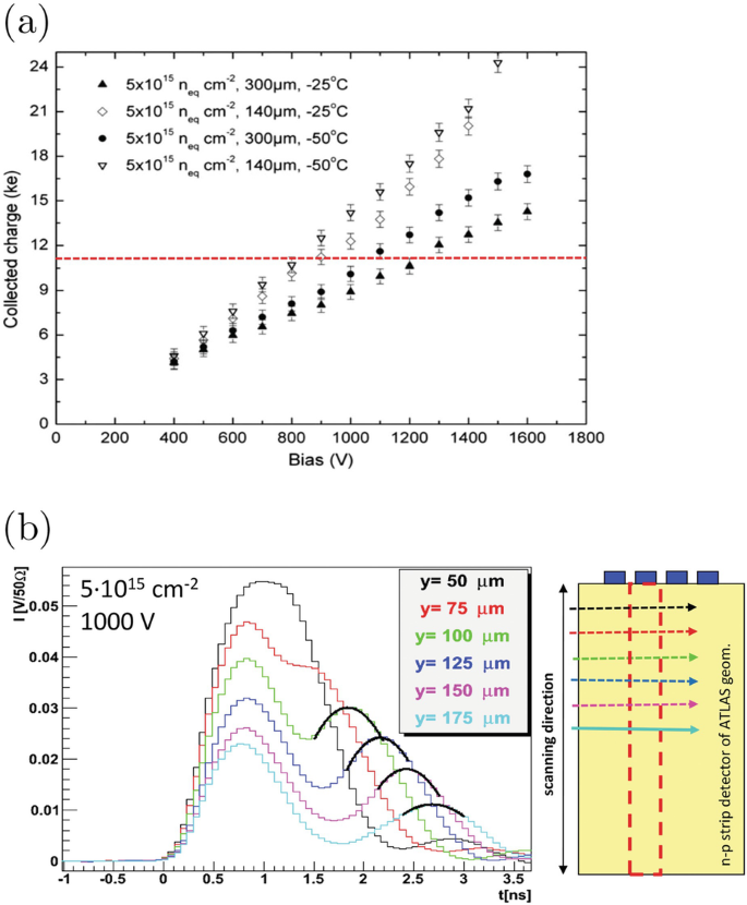
(a) Measured charge collection dependence on voltage for 140 and 300 μm thick strip detectors. The red line denotes the charge measured in non-irradiated 140 μm thick detector. (b) Induced current pulses in strip detector for different depths of Edge-TCT injection. The second peak in the induced current pulses is due to multiplied holes drift
-
Charge gain depends on the hit position within the electrode. In highly irradiated strip detectors higher gain was observed for tracks few μm away from the implant, where the electric fields are highest [60].
-
The holes produced in multiplication are trapped by deep defects (change of free hole concentration, p, in Eq. (21.15)) which reduce the negative space charge—act as a feedback. Therefore gain increases moderately with voltage and is usually limited to factors below <10.
-
Gain can vary on time scale of days when detector is under bias [61].
-
It is difficult to parametrize the field and reliably simulate the operation.

Annealing Performance of Highly Irradiated p-type Detectors
Active bulk and charge multiplication have an important impact on performance of p-type detectors after annealing. Increase of N eff with time and consequent increase of electric field increases gain. On the other hand smaller high field region near the electrodes affects less the performance due to significant field in the neutral bulk. A typical annealing performance is shown in Fig. 21.24a. At lower voltages charge collection increases during short term and decreases during long term annealing (red band), which is in agreement with evolution of effective doping concentration. At higher voltages the charge multiplication compensates the decrease of active region (blue band) and at highest voltages overcompensates it, resulting in smallest charge collection for completed short term annealing (green band). At higher fluences and voltages shown in Fig. 21.24b the beneficial effect of long term annealing is even more pronounced.

Dependence of charge collection on annealing time at 60∘C at different bias voltages at (a) Φeq = 1 ⋅ 1015 cm−2 and (b) Φeq = 5 ⋅ 1015 cm−2 [62]
Noise
The increase of noise due to multiplication can diminish the benefits or even deteriorate the performance in terms of signal/noise ratio. The details about the noise in multiplication mode will be discussed at in the section on electronics.
21.4.2.4 Charge Trapping
The decrease of charge collection efficiency is determined by the trapping term and the product \(\vec {E}\cdot \vec {E_w}\) in Eq. (21.29). At fluences beyond that at LHC the trapping term dominates and ultimately sets the limit of efficient operation. The influence of trapping on charge collection can be clearly seen for a fully depleted detector, where the degradation of the induced charge is exclusively due to trapping. The collected charge degrades with fluence as shown in Fig. 21.25a. The degradation is severe and around half the charge in non-irradiated detector (12000 e 0) are measured at V fd for Φeq ∼ 1015 cm−2. The induced charge increases further for bias voltages larger than V fd. Higher electric field reduces the drift time and by that the influence of trapping term.

(a) Dependence of induced charge on voltage for MCz p-type pad detector irradiated to different fluences. The V fd for each measurement is denoted by vertical bar. (b) Effective trapping times of electrons and holes as found in Ref. [64]
If the deep levels responsible for trapping are constant in time or change with a first order process (see Eq. (21.5)), then at any time after irradiation their concentration is linearly proportional to the fluence. Under this assumption Eq. (21.19) can be rewritten as
where β e,h is called effective electron and hole trapping damage constant which depends on temperature, time after irradiation and irradiation particle. In detector grade silicon the effective trapping probability of a non-irradiated detector \(\frac {1}{\tau _{{eff0}_{e,h}}}\) is negligible and is usually omitted from Eq. (21.35). Alternatively the trapping distance can be defined as
measuring the distance the carriers drift before being trapped.
The trapping times in silicon were systematically measured with Transient Current Technique [63]. The trapping probabilities for 23 GeV protons are shown in Fig. 21.25b. At Φeq ∼ 1015 cm−2 the effective trapping times are around few ns.
The trapping damage constant was studied as a function of different material properties: resistivity, oxygen concentration, carbon concentration, wafer production (MCz, FZ, epi-Si) and type of silicon (p-type or n-type). It was found, within the error margin, not to depend on any, thus being universal for silicon. The average values of β for neutrons and charged hadrons are given in the Table 21.5 [65]. It shows that the trapping probability for electrons is smaller than for holes. The NIEL hypothesis is slightly violated as charged hadrons produce more damage than reactor neutrons.
The evolution of trapping probability with time after irradiation is described in the simplest model by the decay of the dominant trap to another dominant trap (Eq. (21.3)) or a model with two traps one constant in time and one that decays. Both models can be described by the following equation [63]
with \(\beta _{0_{e,h}}\) and \(\beta _{\infty _{e,h}}\) the trapping rates at early and late annealing times, respectively. For the annealing temperatures of interest β 0 is very close to β measured at the end of short term annealing (β(t min)) given in Table 21.5. There is a distinctive difference between annealing of effective trapping times for holes and electrons. The trapping probability of holes increases with annealing time and that of electrons decreases (see Fig. 21.26) irrespective of material properties and type of irradiation particle. The parameters describing annealing of effective trapping probabilities are shown in Table 21.6. The activation energy E ta should be used in Eq. (21.9) for scaling τ ta to different temperatures. The β e,h depends only moderately on temperature [63]. At temperatures of interest for most applications the trapping probabilities for both holes and electrons decrease with temperature by around 10–20% if the temperature changes from − 20∘ to 20∘C.

Annealing of 1∕τ eff,e,h for a detector irradiated with neutrons to Φeq = 1.5 ⋅ 1014 cm−2
The linear relation of Eq. (21.35) breaks down at equivalent fluences higher than ∼1015 cm−2, where it starts to exhibit saturation. Unfortunately the TCT can not be directly used to measure trapping probabilities and values have be extracted by combining both TCT and CCE measurements with simulations. The study performed by CMS collaboration is shown in Fig. 21.27 [66]. It can be seen that already at few times 1015 cm−2 the effective trapping probabilities deviate significantly from linear. Recently studies [67] showed that at extreme fluences of ∼1017 cm−2 the trapping probability is around an order of magnitude smaller than predicted from the low fluence measurements.

21.4.2.5 Generation Current
The defects influencing the generation current (Eq. (21.22)) were found to either dissociate or are constant in time. The bulk damage-induced increase of the reverse current (ΔI) exhibits therefore a simple dependence on particle equivalent fluence at any time after irradiation
where V is the active volume (V = Sw) and α the leakage current damage constant. The bulk generation current scales with NIEL, hence the leakage current damage constant is independent of the silicon properties and irradiation particle type as shown in Fig. 21.28a [68]. The measured value of the leakage current depends exponentially on the operating temperature as (see terms in Eq. (21.22))
and accordingly all α-values can be scaled to any temperature.

(a) Dependence of bulk generation current on fluence for different detectors after 80 min storage at 60 ∘C. (b) Annealing of leakage current damage constant (after [31])
The damage induced bulk current undergoes also a temperature dependent beneficial annealing, described by
with α 0 = 5.03 ⋅ 10−17 A/cm, α 1 = 1.01 ⋅ 10−17 A/cm, α 2 = 3.34 ⋅ 10−18 A/cm, τ α = 93 min and t norm = 1 min all measured at 60 ∘C. The first term in the Eq. (21.40) describes the decay of the defect and the second contribution of the defects constant in time. The last term is associated with the decay of the cluster, a conclusion based on its absence in 60Co irradiations [68]. The leakage current annealing can be seen in Fig. 21.28b. Universality of the annealing described by Eq. (21.40) can be used to reliably monitor the equivalent fluence of particle sources even in cases of wide energy distributions. As a standard α(80 min at 60∘C, 20∘C) = 4 ⋅ 10−17 A cm−1 is used.
21.4.2.5.1 Leakage Current in Presence of Charge Multiplication
For devices with gain the leakage current is given by the current gain M Footnote 2 and generation current I = M ⋅ I gen. An example of the leakage current increase at high bias voltages during annealing is shown in Fig. 21.29. One should however be careful as the increase of leakage current at high bias voltages can also be attributed to other effects such as the onset of thermal runaway or rise of the surface current, however without clear increase of the collected charge.

Dependence of leakage current on annealing time at different voltages. The increase of leakage current with annealing is due to charge multiplication (from Ref. [62])
21.4.2.6 Alternative Ways of Operation
The key reason for changes in performance of an irradiated detector are deep traps. The manipulation of their occupancy therefore has an influence on the detector properties. Variation of the operation temperature and/or concentration of free carriers can be used to change the occupancy of deep traps. The first observation of charge collection efficiency recovery after gradually cooling down the heavily irradiated silicon detector from room temperature to cryogenic temperatures (see Fig. 21.30a) was reported in [69] and referred to as “Lazarus effect”. However the operation of silicon detectors under reverse bias turned out to be very sensitive to previous biasing conditions and ionizing particle rates. The signal varies with time after exposure to ionizing particles as shown in Fig. 21.30b. The trapping of the drifting carriers enhances the space charge of different signs at both detector contacts (see Sect. 21.4.2.2) to the point where the applied voltage is insufficient to establish the electric field in the entire detector. As a consequence the charge collection efficiency is reduced. The phenomena of polarization of the detector by trapped charge is not unique to silicon and is present also in other semiconductors. Since emission times depend on E g∕(2 k BT), silicon at cryogenic temperatures behaves similarly as wide band gap semiconductors at room temperature.

(a) Charge collection efficiency in 400 μm thick detector irradiated to 1015 cm−2 in forward and reverse direction. (b) The dependence of CCE on voltage at T = 77 K in both forward and reverse direction of a detector irradiated to 2 ⋅ 1015 cm−2
At cryogenic temperatures a more stable operation is achieved with detectors biased in forward direction [70] (see Fig. 21.30a,b). The resistivity of the bulk increases with irradiation and it effectively becomes a heavily doped insulator. Applied bias in forward direction injects carriers in the detector. These are trapped at deep levels and affect the electric field. The predominately negative space charge is naturally compensated by injection of holes. The electric field grows from E ≈ 0 at the injection point towards the other contact with the square root of the distance x from the injecting junction [71]
The electric field extends through the entire detector thickness regardless of the applied voltage or concentration of the deep levels. This is an important advantage over the biasing of detectors in reverse polarity. The drawback of forward bias operation is the increased current, requiring intensive cooling. The current dependence on voltage is quadratic (I ∝ V 2), followed by a sharp rise at threshold voltage V T as shown in Fig. 21.31. It happens when the space charge saturates due to filling all the traps and current can not be limited by increasing the concentration of the trapped carriers, therefore V T ∝ Φeq. An important feature of this mode of operation is the fact that the current at a given voltage progressively decreases with fluence (see Fig. 21.31), approximately as \(I(\Phi _{eq})\propto \Phi _{\mathrm {eq}}^{-1.5}\). The larger the concentration of traps the smaller is the current which is needed to adjust the electric field. Nevertheless, it is still larger than in reverse direction.

Leakage current-voltage characteristics in forward mode of operation
In principle, a p + − n − n + structure should inject holes and electrons, which would not produce the aforementioned properties. However it turns out that at n + contacts electrons are not injected [71]. The symmetric structure p + − n − p +, where only holes are injected, has the same properties pointing to the same underlying physics process. The same condition of carrier injection can be also achieved in reverse bias mode by continuous illumination of one side by light of short penetration depth [72]. The injected carries establish the same condition as under forward bias and the Eq. (21.41) applies.
The filling of deep levels affects effective trapping probabilities of electrons and holes. Measurements have shown that the same charge collection efficiency is achieved as for a fully depleted detector at few times smaller bias voltage [70, 73] (see Fig. 21.30b). Smaller bias results in smaller average electric field and therefore longer collection times. As the reduction of charge collection efficiency depends in first approximation on the ratio of the drift time to the trapping time of the carriers, the latter must be longer than under the reverse bias.
It is obvious that forward bias operation mode becomes usable once the detectors are already heavily irradiated. There are two ways of how to use detectors in real experiments. With read-out electronics sensitive to both polarities detectors can be first used in reverse and later in forward direction or the detectors are irradiated before being used. In general the use of the forward bias means replacing the problem of the high voltage required for the reverse bias operation by the problem of a high dark current. Therefore detectors with small element size (i.e. pixels) are more suitable for this mode of operation.
21.4.2.7 3D Detectors—A Radiation Harder Detector Design
One approach to address the issue of radiation damage are optimized detector geometries. A good example of radiation hard detector design are so called 3D detectors. An schematic view of such detector is shown in Fig. 21.32 [74]. The electrodes in such detectors are perpendicular to the surface. Such placement of electrodes has two beneficiary effects for heavily irradiated detectors. The small distance between the electrodes effectively reduces the full depletion voltage. Even more importantly, the drift length of carriers is reduced and therefore the probability of drifting carriers to get trapped (τ eff,e,h ≫ t drift). As the signal (number of e-h pairs in Eq. (21.29)) is determined by the detector thickness, vertical electrode configuration ensures good charge collection at moderate voltages. Several columns can be connected together to form pixel cells or strips (Fig. 21.32b). The thickness of the detector is limited by the deep reactive ion etching process used to produce holes. The standard aspect ratio (hole length/hole diameter) is around 24. Apart from a more complex processing, which can be simplified by electrodes not penetrating fully the detector [75, 76], there are some drawbacks of the 3D design:
-
Reducing the inter-column spacing results in higher inter-electrode capacitance
Fig. 21.32 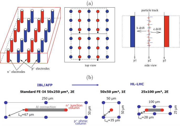
(a) The schematic view of the 3D detector (left). The view of the detector surface (middle); gray n + electrodes, dark gray p + electrodes, black metal line, black dot the bump-bond. The dashed line marks the pixel cell with three columns. \(Q_e^t/Q^t\) for different tracks: p1=1, p2=0.5 in p3=0 (right). (b) Layout of a single cell/pixel of an IBL 3D detector (2 electrode configuration—2E) and of HL-LHC detector with both options 1E and 2E. The maximum drift length of carriers is indicated
-
Columnar electrodes are a non-active part of the detector volume and can lead to particle detection inefficiency; most of the tracks in experiments are, however, inclined which mitigates the problem.
-
Induced charge depends on the hit position of the particle track. Unlike in planar detectors, the ratio \(Q_e^t/Q^t\) varies between 0 and 1 across the detector and can affect the position resolution and efficiency (see Fig. 21.32c).

Nevertheless, these detectors are often first choice for tracking detectors at highest fluences. ATLAS pixel detector (Insertable B Layer—IBL) [77] saw the first application of 3D detectors for tracking in high energy experiments, covering 25% of the total IBL surface at both sides of the staves. The 3D technology is improving with different ways of processing the detectors with single-sided process or more elaborate double sided processing with possibility of active/slim edges reducing the inactive part at the detector border. Efficient charge collection was achieved also for sensors where columns don’t penetrate the whole depth. Such a design improves the yield of sensor production. The latter remains one of the main concerns for 3D technology reaching around 50–60% for the IBL module production [78].
At HL-LHC the 3D detectors are planned for the first pixel layer. A small cell size will have a single junction column (cell 50 × 50μm2) or two columns (cell 25 × 100 μm2), where the maximum drift distances will be reduced to mere 37 and 28 μm making these detectors extremely radiation hard. The first beam tests with such 230 μm thick detectors showed [79] 97% detection efficiency for perpendicular tracks after extreme fluences of 2.5 ⋅ 1016 cm−2 at >200 V using IBL readout electronics (FE-I4) [80].
21.4.2.8 Timing Detectors
At HL-LHC coping with large particle fluxes emerging from collisions will be an enormous challenge. On average 200 p-p collisions will occur every 25 ns, with collision points distributed normally along the beam with σ z = 5 cm and in time with σ t = 180 ps. Resulting track and jet densities in the detector complicate the analysis of the underlying reactions that took place. A way to cope with that problem is separation of individual collisions also in terms of time of occurrence within each bunch crossing. This is particularly important for tracks/jets in forward direction for which the position resolution of primary vertex is much worse (∼1 mm). If tracks are not resolved in time, this can lead to false vertex merging. A timing resolution of around 30 ps with respect to the HL-LHC clock is required to successfully cope with pileup. Such an outstanding single particle timing resolution was up to recently impossible with silicon detectors.
Three factors determine the timing resolution of each sensor: time walk which is a consequence of non-homogeneous charge deposition by an impinging particle, noise jitter (σ jitter = t rise∕(S∕N)) and resolution of time-to-digital conversion. Standard silicon detectors of 300 μm are not appropriate for precise timing measurement as the integration time to collected all the charge and consequent rise time t rise are large, hence the jitter. In addition fluctuations, not only of the amount of the charge (time walk correctable by e.g. constant fraction discrimination), but also of the deposition pattern (non-correctable time walk)—so called Landau fluctuations—ultimately limit the time resolution to effectively >100 ps [81]. High enough signal-to-noise S∕N in thin detectors can be achieved by using so called Low Gain Avalanche Detectors (LGAD) [82].
They are based on a n ++ − p + − p − p ++ structure where an appropriate doping of the multiplication layer (p +) leads to high enough electric fields for impact ionization (see Fig. 21.33) [82]. Gain factors in charge of few tens significantly improve the resolution of timing measurements, particularly for thin detectors. The main obstacle for their operation is the decrease of gain with irradiation, attributed to effective acceptor removal in the gain layer [41]. A comprehensive review of time measurements with LGADs is given in Ref. [83].

Schematic view of the Low Gain Avalanche Detector
The most probable charge in 50 μm and 80 μm thick pad devices before and after irradiation is shown in Fig. 21.34a. As soon as multiplication layer is depleted the gain appears. At lower fluences the gain degradation at the depletion of multiplication layer (around 40 V) can be clearly seen. At higher fluences the gain appears at high bias voltages where over-depletion ensures that high enough electrical fields are reached; above Φeq > 1015 cm−2 the onset of multiplication is observed only at highest voltages of around 700 V. Such voltages correspond to very high average fields of 15 V/μm. At fluences Φeq > 2 ⋅ 1015 cm−2 the beneficial effect of multiplication layer is gone. The devices of the same design without multiplication layer show similar behavior as LGADs. The time resolution of LGADs was extensively measured in the test beams [84] and with 90Sr electrons. It is shown in Fig. 21.34b for the 50 μm thick non-irradiated devices.

Dependence of most probable charge for irradiated LGAD devices on voltage for different thickness (50 and 80 μm). Fluences in the brackets are in [cm−2] [85]. Around 3000 e is expected for a 50 μm device without gain layer. (b) Time resolution and its noise jitter contribution measured for the non-irradiated 50 μm detector at different temperatures [86]
At very large fluences of Φeq > 2 ⋅ 1015 cm−2 the gain, although lower than the initial, appears due to deep traps (see section on charge multiplication) and the timing resolution degrades only moderately (see Fig. 21.35a). Moreover, multiplication in larger volume of the bulk results in faster rise time of the induced current which at given gain leads to better timing resolution (see Fig. 21.35b).

(a) Time resolution of irradiated LGAD detectors at different gains and fluences ([cm−2]). (b) Measured and simulated induced current pulse shape at different irradiation levels. Note that amplitudes were normalized to one
The leakage current in LGADs follows the same equation as discussed in section on charge multiplication. Hence, the gain can be calculated from measurement of leakage current and calculated generation current [85, 86].
A lot of effort was spend in recent years to increase the radiation hardness of LGADs by mitigating the acceptor removal. The efforts concentrated to use of co-implantation of carbon [87] to multiplication layer aiming to reduce the removal constant or replacing boron with gallium, which should be more difficult to displace [87, 88].
21.4.3 Diamond Detectors
Although the specific ionization in diamond detectors is around three times smaller than in silicon, larger detector thickness, small dielectric constant, high break down voltage and negligible leakage current make them the most viable replacement for silicon in the highest radiation fields.
The intrinsic concentration of carriers in diamond is extremely low (good insulator, ρ > 1016 Ωcm). The detectors are therefore made from intrinsic diamond metallized at the back and the front (see Fig. 21.36) to form ohmic contacts. Most of the diamond detectors are made from poly-crystalline diamond grown with chemical vapor deposition technique (CVD). Recently also single crystalline (scCVD) detectors have become available. The quality of the poly-crystalline (pCVD) diamond as a particle detector depends on the grain size. The grains in this material are columnar, being smallest on the substrate side, and increasing in size approximately linearly with film thickness.Footnote 3 Crystal faults at the boundaries between the grains give rise to states in the band gap acting like trapping centers.

Schematic view of the pCVD diamond detector
A widely used figure of merit for diamond is its charge collection distance (CCD), which is defined as
The CCD represents the average distance over which carriers drift. If CCD ≪ W, it is equivalent to the trapping distance λ e + λ h.Footnote 4. After irradiation, and for pCVD detectors also before irradiation, the CCD depends on electric field, due to reduced probability for charge trapping at larger drift velocity. Only for non-irradiated scCVD detectors λ e,h →∞ and the CCD = W regardless of the bias voltage applied. Most commonly, the CCD is defined at E = 1 V/μm or E = 2 V/μm, although sometimes also CCD at saturated drift velocity is stated.
The CCD of typically 500 μm thick diamond detectors has improved tremendously over the last 20 years. Current state of the art pCVD detectors reach up to 300 μm at 2 V/μm and are available from 6 inch wafers.
21.4.3.1 Radiation Hardness
In pCVD detector the leakage current does not increase with irradiation; moreover it may even decrease, which is explained by passivation of defects at grain boundaries. The current density in high quality pCVD diamond is of order 1 pA/cm2, a value strongly dependent on the quality of metallized contacts.
Irradiation decreases the CCD for both scCVD and pCVD diamonds with similar rate [89], pointing to the in-grain defects being responsible. It has been observed that exposing such an irradiated detector to ionizing radiation (1010 minimum ionizing particles/cm2) improves the charge collection efficiency of pCVD detectors by few 10%. This process is often called “pumping” or priming. The ionizing radiation fills the traps. The occupied traps become inactive, hence the effective trapping probability decreases. The traps can remain occupied for months due to large emission rates if kept in the dark at room temperatures. Once detectors are under bias the ionizing radiation leads to polarization of detectors, in the same way as in silicon, but with the polarization persisting over much longer times. The measurements of charge collection can therefore depend on previous biasing condition and relatively long times are needed to reach steady state of operation.
The irradiation decreases the trapping distance of electrons and holes proportionally to the fluence. The relation can be derived by inserting the effective trapping time (Eq. (21.35)) in the expression for the trapping distance (Eq. (21.36)):
where λ 0 denotes the trapping distance of an unirradiated detector and K e,h the damage constant. Assuming λ e ≈ λ h and λ e + λ h ≪ W for simplicity reasons, CCD dependence on fluence can be calculated as:
Although only approximate the Eq. (21.44) fits the measurements well over a large fluence range as shown in Fig. 21.37a. The extracted damage constant K (∼1∕2 K e,h) from source and test beam data for particles of different energy and spectrum are gathered in Table 21.7. For high fluences the second term in Eq. (21.44) prevails and the scCVD and pCVD diamonds perform similarly. At Φ = 2 ⋅ 1016 cm−2 of 23 GeV protons the CCD ≈ 75 μm which corresponds to mean charge of 2770 e 0. At lower fluences the first term dominates and for CCD 0 ∼ 200 μm CCD only decreases by 15% after 1015 cm−2 of 23 GeV protons.

(a) CCD vs. fluence of different particles. Detectors were 500 μm thick. The Eq. (21.44) is fitted to the data [89,90,91]. The irradiation particle, electrode geometry and electric field is given in brackets. (b) Energy loss distribution in CVD pad detectors. The value of FWHM, corrected for electronics noise, over most probable energy loss is shown
The homogeneity of the response over the detector surface, which is one of the drawbacks of pCVD detectors, improves with fluence for pCVD as the collection distance becomes smaller than grain size. For the same reason also the distribution of energy loss in pCVD detector, initially wider than in scCVD, becomes narrower (Fig. 21.37b). The energy loss distribution in pCVD diamond is Gaussian, due to convolution of energy loss distributions (Landau) in grains of different sizes.
One of the main advantages of the diamond is the fact that at close to room temperatures no annealing or reverse-annealing effects were observed.
The drawbacks of grains in pCVD detectors can be largely overcome by using 3D diamond detectors [93], who share the same concept with silicon detectors (see Fig. 21.38). The vertical electrodes are produced by focused laser light which graphitizes the diamond. Whether the vertical electrode serves as cathode or anode depends on metal bias grid on the surface of the detector. Very narrow electrodes of ∼2 μm diameter can be made along 500 μm thick device with low enough resistivity to allow good contacts and doesn’t increase the noise. Such a good aspect ratio allows even smaller cell sizes than in silicon.

Photograph of 3D diamond strip detector in black rectangle with a square cell of 150 μm size. Strip detector of the same geometry with planar electrodes is shown below (from [93])
The first tests showed >75% charge collection efficiency in 500 μm pCVD diamond detector of ganged 150 × 150μm2 cells with bias voltages of only few tens Volts [94]. A much better homogeneity of charge collection over the surface (columns are parallel to grain boundaries) and narrower distributions of collected charge were obtained than in planar diamond detectors.
The main problem with diamond 3D detectors is the rate of production in particular for large area as even if laser beam is powerful enough and is split into several parallel beams. Currently the rate is limited to roughly ten thousand holes a day.
The diamond detectors are used also outside particle physics for particle detection such as for fusion monitoring where neutrons are detected, for alpha particle detection, for determination of energy and temporal distribution of proton beams and in detection of ions during the teleradiology. They are also exploited for soft X-ray detection, where the solar-blindness and fast response of diamond detectors are the keys of their success.
21.4.4 Other Semiconductor Materials
Silicon is in many respects far superior to any other semiconductor material in terms of collected charge, homogeneity of the response and industrial availability. Other semiconductor materials can only compete in niche applications where at least one of their properties is considerably superior or where the existing silicon detectors cannot be used. For example, if low mass is needed or active cooling can not be provided, high leakage current in heavily irradiated silicon detectors is intolerable and other semiconductor detectors must be used.
The growth of compound semiconductors is prone to growth defects which are frequently unmanageable and determine the properties of detectors before and after irradiation. If a high enough resistivity can be achieved, the detector structure can be made with ohmic contacts. However, it is more often that either a Schottky contact or a rectifying junction is used to deplete the detector of free carriers. Only a few compound semiconductors have reached a development adequate for particle detectors. They are listed in the Table 21.2. For particle physics application some other very high-Z semiconductor such as CdZnTe or HgI2 are inappropriate due to large radiation length.
Silicon Carbide
was one of the first alternatives to silicon proposed in [95, 96]. It is grown as epitaxial layer or as bulk material. Even though at present the latter exhibits a lot of dislocations (inclusions, voids and particularly micro-pipes) in the growth and the former is limited to thicknesses around 50 μm, both growth techniques are developing rapidly and wafers are available in large diameters (10 inch). Due to the properties similar to diamond the same considerations apply as for diamond with an important advantage of 1.4 larger specific ionization (55 e-h/μm).
Presently the best performing detectors are produced by using slightly n-doped epitaxial layers of ≈50 μm forming a Schottky junction.They exhibit 100% charge collection efficiency after full depletion and negligible leakage current [97]. Also detectors processed on semi-insulating bulk (resistivities ∼1011 Ωcm) with the ohmic contacts show CCD up to 40 μm [96] at 1 V/μm for few hundred μm thick material.
After irradiation with hadrons the charge collection deteriorates more than in silicon or in diamond. For epitaxially grown SiC the degradation of CCD is substantial with K e ≈ 20 ⋅ 10−18 cm2/μm and K h ≈ 9 ⋅ 10−18 cm2/μm for reactor neutron and 23 GeV p irradiated samples at high electric fields of 10 V/μm [97, 98]. The leakage current is unaffected by irradiation or it even decreases [98].
GaAs
The resistivity of GaAs wafers is not high enough for the operation with ohmic contacts and detectors need to be depleted of free carriers, which is achieved by Schottky contact or a p − n junction. GaAs detectors were shown to be radiation hard for γ-rays (60Co) up to 1 MGy [99]. As a high Z material these detectors are very suitable for detection X and γ rays.
Their tolerance to hadron fluences is however limited by loss of charge collection efficiency, which is entirely due to trapping of holes and electrons. The V fd decreases with fluence [100, 101] which is explained by removal or compensation of as grown defects by irradiation. Although larger before the irradiation, the trapping distance of electrons shows a larger decrease with fluence than the trapping distance of holes. The degradation of charge collection distance at an average field of 1 V/μm (close to saturation velocity) in 200 μm thick detectors is very large K e,π ≈ 30 ⋅ 10−18 cm2/μm and K h,π ≈ 150 ⋅ 10−18 cm2/μm [100]. One should however take into account that specific ionization in GaAs is four times larger than in diamond.
The leakage current increases moderately with fluence up to few 10 nA/cm2, much less than in silicon, and starts to saturate at fluences of around 1014 cm−2 [100, 101]. The GaAs exhibit no beneficial nor reverse annealing of any detector property at near to room temperatures.
GaN
The GaN detectors produced on few μm thin epitaxial layer shown charge collection degradation which is much larger than in Si [102]. Further developments in crystal growth may reveal the potential of material.
21.4.5 Comparison of Charge Collection for Different Detectors
The key parameter relevant to all the semiconductor particle detectors is the measured induced charge after passage of minimum ionizing particles. The charge collection dependence on fluence in different semiconductor pad detectors is shown in Fig. 21.39a. A 3D pad detector (all columnar electrodes connected together) shows best performance, while smallest charge is induced in SiC and pCVD diamond detectors. The induced charge decreases with fluence and at most few thousand e 0 can be expected at Φeq > 1016 cm−2.

(a) Comparison of charge collection in different detectors and materials; given are material, thickness, voltage, [shaping time of electronics and temperature]. “od.” means at V bias > V fd. All detectors were irradiated with 23 GeV protons, except 75 μm epi-Si and 300 μm thick “spaghetti” diode which where irradiated with reactor neutrons. For diamond detectors the mean, not the most probable, charge is shown. (b) Charge collection in different segmented devices; the segmentation is denoted for strips (thickness-pitch-width) and pixels (thickness-cell size)]. Solid markers denote neutron irradiated and open 23 GeV proton irradiated samples
Although pad detectors are suitable for material comparison the effect of segmentation and choice of the type of the read-out electrodes determine to a large extent the performance of the detectors. The superior charge collection performance of segmented silicon planar detectors with n + electrodes to pad detectors can be seen in Fig. 21.39b. A signal of around 7000 e 0 is induced in epitaxial p-type and Fz p-type strip detectors at Φeq = 1016 cm−2. At the highest fluence shown the signal in a silicon pad detector is only half of that in a strip detector. On the other hand a device with p + readout performs worst of all.
The detection efficiency, however, depends on signal-to-noise ratio, which should be maximized. A choice of material, electrode geometry and thickness determine the electrode capacitance which influences the noise of the connected amplifier (Chap. 10). At given pixel/strip geometry the highest electrode capacitance has a 3D silicon detector, followed by a planar detector with n + electrodes, due to required p-spray or p-stop isolation which increases the inter-electrode capacitance. Even smaller is the capacitance of p + electrodes which is of 1 pF/cm order for strip detectors. The smallest capacitance is reached for diamond detectors owing to small dielectric constant.
21.4.5.1 Operation at Extreme Fluences
A combination of trapping times saturation, active neutral bulk and charge multiplication allows silicon detectors to be efficient in radiation environments even harsher than that of HL-LHC, approaching those of FCC. The operation of silicon detectors was tested up to Φeq = 1.6 ⋅ 1017 cm−2 and is shown in Fig. 21.40a for short strip detectors with ganged electrodes (“spaghetti” diode). Detectors remained operational and most probable charge of around 1000 e was measured in 300 μm thick detectors at 1000 V. At high fluences (>2 ⋅ 1015 cm−2) the collected charge is linearly proportional with o bias voltage in whole range of applicable voltages and the dependence of charge on voltage and fluence can be parametrized with only two free parameters [103],
where b = −0.683 and k = 26.4 e∕V for 300 μm thick detectors.

(a) Dependence of collected charge in different planar silicon detectors on voltage up to the extreme fluences at − 10∘C. The color bands are to guide the eye. (b) Test beam (120 GeV π) measurement of detection efficiency in heavily irradiated 3D detector with single electrode cell of 50 × 50μm2 shown in the inset [79]
A small cell size 3D detector (50 × 50μm2, 1E) irradiated with charged hadrons to Φeq = 2.5 ⋅ 1016 cm−2 was recently found to be fully efficient at voltages even below 200 V (see Fig. 21.40b) [79]. A rough simulation of collected charge in such a device based on known data predicts collected charge >3000 e0 after the fluence of 1017 cm−2, which may be already enough also for successful tracking.
21.4.6 Radiation Damage of Monolithic Pixel Detectors
The monolithic pixel detectors, which combine active element and at least first amplification stage on the same die, are widely used in x-ray and visible imaging applications. Their use as particle detectors is limited for applications where radiation environments are less severe (space applications, e + − e − colliders), either because of small hadron fluences or because of radiation fields dominated by leptons and photons (see Fig. 21.3). The CCD is the most mature technology while CMOS active pixel sensors were successfully used for particle detection in STAR experiment at Relativistic Heavy Ion Collider over the last decade. These detectors are more susceptible to radiation damage due to their charge collection mechanism and the readout cycle. Recently several CMOS foundries offered a possibility to apply high voltage which can be used for depletion of substrate on which CMOS circuitry resides thereby enabling fast charge collection by drift. This greatly enhanced both radiation hardness of CMOS detectors and their speed.
The principles of operation of these detectors were addressed in section on Solid state detectors. Here on only the aspects of radiation hardness of aforementioned detectors will be addressed.
21.4.6.1 CCDs
The CCDFootnote 5 is intrinsically radiation soft. The transfer of the charge through the potential wells of the parallel and serial register is very much affected by the charge loss. At each transfer the fraction of the charge is lost. The charge collection efficiency is therefore calculated as CCE = (1 − CTI p)n × (1 − CTI s)m, where CTI s and CTI p denote the charge collection inefficiency of each transfer in serial and parallel register. An obvious way of improving the CCE is a reduction of the number of transfers (m and n). Applications requiring high speed such as ILC, where the readout of the entire detector (n ∼ 2500) within 50 μs is neeeded, the serial register is even omitted (m = 0) and each column is read-out separately (column parallel CCD [104]). The CCDs suffer from both surface and bulk damage.
The increase of CTI is a consequence of bulk and interface traps. There are several methods to improve the CTI:
-
The transport of the charge takes place several hundred nm away from the surface by using a n + implant (buried channel), which shifts the potential minimum. The transport is less affected by trapping/detrapping process than at the interface traps.
-
Operation of CCDs at low temperatures leads to filling of the traps with carriers—electrons. Since emission times are long (Eq. (21.16)) the amount of active traps is reduced.
-
If the density of signal electrons (n s) is larger than the trap concentration only a limited amount of electrons can be trapped, thus CTI ∝ N t∕n s. An additional n + implant can be used for buried channel CCDs to squeeze the potential minimum to much smaller volume (see Fig. 21.41).
Fig. 21.41 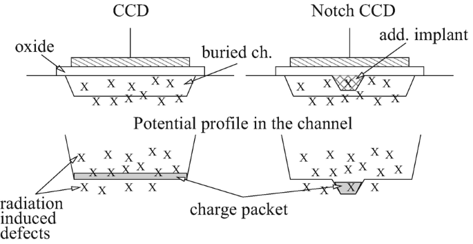
The principle of notch CCD. An additional n + implant creates the minimum in potential
-
The CTI depends on the charge transfer timing, i.e. on the clock shapes. The transfer of the charge from one pixel to another should be as fast as possible to reduce the trapping. The choice of the clock frequency, number of the phases (2 or 3) and shape of the pulses, which all affect the CTI, is a matter of optimization (see Fig. 21.42). The transfer time from one well to another can be enhanced by an implant profile which establishes gradient of the electric field.
Fig. 21.42 
Comparison of charge transfer of 2 and 3 phase CCD (P1,P2,P3 denote gate drive voltages). Note that the potential well occupies 1/4 of the pixel volume for 2 phase CCD and up to 2/3 for 3-phase CCD. The signal charge is shaded
-
If traps are already filled upon arrival of the signal charge they are inactive and CTI decreases. The effect can be achieved either by deliberate injection of charges (dark charge) or by exploiting the leakage current. In the same way also the pixel occupancy affects the CTI.


The radiation affects also operation of detectors due to surface effects. The surface generation current which is a consequence of interface traps is in most of the applications the dominant source of current in modern CCDs. Very rarely the bulk damage is so high that the bulk generation current dominates. The surface dark current can be greatly suppressed by inverse biasing of the Si-SiO2 interface [105].
The voltage shift due to oxide charge requires proper adjustment of the amplitude of the gate drive voltages. However the supply current and power dissipation of the gate drivers can exceed the maximum one as they both depend on the square of the voltage amplitude.
The CCDs can probably not sustain radiation fields larger than at the ILC (see Table 21.1), particularly because of the bulk damage caused by neutrons and high energy leptons.
21.4.6.2 Active CMOS Pixels
In conventional monolithic active CMOS pixel sensors (Chap. 5) [106, 107] the n + well collects electron hole pairs generated by an ionizing particle in the p doped epitaxial layer (see Fig. 21.43). The built-in depletion around the n + well is formed enabling the drift of the carriers. In the major part of the detector the charge is collected from epitaxial p-type silicon through the diffusion. The charge collection process depends on epitaxial layer thickness and takes tens of ns. Above 90% of the cluster charge is induced within ∼100 ns for 15 μm thick epitaxial layer [108]. Since the n + wells are used as collection electrodes, only nMOS transistors can be used for the signal processing circuit. The level of complexity of signal processing after the first stage depends on the CMOS technology used (number of metal layers, feature size).

Schematic view of the radiation effects in active CMOS Pixel Detector: (1) generation of carriers—leakage current; (2) recombination of diffusing carriers; (3) positive oxide charge buildup leads to punch trough the p well; (4) charge trapping at shallow trench isolation structure
The charge collection by thermal diffusion is very sensitive to electrons lifetime, which decreases due to the recombination at deep levels. The loss of collection efficiency and consequently smaller signal-to-noise ratio is the key limitation for their use. The way to increase the radiation tolerance is therefore the reduction of diffusion paths. This can be achieved by using many n + collection diodes per pixel area, which improves the charge collection efficiency. The price for that is a larger capacitance and leakage current of the pixel. An increase of the epitaxial layer will increase the fraction of recombined charge, but the absolute collected charge will nevertheless be larger. The reduction of the collection time can be achieved by a gradual change of epitaxial layer doping concentration which establishes electric field.
The generation-recombination centers give rise to the current and cooling is needed to suppress it. It increases the noise and requires more frequent reset of the pixel.
The active pixel detectors were proven to achieve detection efficiencies of >95% at Φeq = 2 ⋅ 1012 cm−2 [109], suggesting an upper limit of radiation tolerance to hadron fluences of Φeq ≤⋅1013 cm−2.
The active pixel sensors are CMOS circuits and therefore susceptible to surface damage effects. Apart from the damage to transistor circuitry which is discussed in next section in some CMOS processes the n-well is isolated from p-well by shallow trench SiO2 isolation. The radiation induced interface states serve as trapping centers and reduce the signal. The active pixel sensors were shown to be tolerant to ionizing radiation doses of up to 10 kGy [110]. The damage effects discussed above are shown in Fig. 21.43.
21.4.6.2.1 Depleted CMOS
In recent years a so called depleted CMOS or high voltage CMOS (HV-CMOS) process has become available by different foundries. These processes allow application of high voltage to the p substrate which becomes depleted. Charge collection by drift significantly improves both speed and radiation tolerance of these devices. The devices differ mostly in the way the collection electrode is realized. A small n + collection electrode is beneficial (see. Fig. 21.44a) for its small capacitance. If, however, a n + electrode is inside a large n-well the capacitance is determined by the size of n-well (see. Fig. 21.44b), but the charge collection is faster and more homogeneous. The optimum design therefore depends on the application (see Ref. [112]). Both options are under consideration for the upgrade of pixel sub-detectors at HL-LHC.

Schematic view of (a) small electrode and (b) large electrode HV-CMOS detectors [111]
Relatively high doping concentration of the substrate (from N eff = few 1012 to 1015 cm−3) emphasizes the importance of effective acceptor removal with irradiation. For low resistivity substrates the removal of shallow acceptors dominates over the creation of deep ones and the effective doping concentration initially decreases with irradiation. The active/depleted thickness at given voltage increases resulting in larger collected charge. After the initial acceptors are removed the deep acceptors determine the depleted thickness regardless of the choice of initial substrate. The dependence of N eff on fluence for different initial substrate resistivities/doping is shown in Fig. 21.45a [37]. The increase of active thickness is reflected also in charge collection measurements shown in Fig. 21.45b for a low resistivity, 20 Ωcm, device. Note that after the irradiations the contribution from the charges diffusing from the undepleted substrate to the depleted region vanishes and almost no charge is measured without bias. The contribution of carriers diffusing from the undepleted substrate disappears already after Φ ∼ 1014 cm−2 [36] which is the reason for initial drop of charge collection efficiency.

(a) Dependence of substrate N eff on fluence of devices produced by two different foundries on different substrate resistivities. Fit of Hamburg model to the data is shown with initial acceptor removal parameters left free [37]. (b) Charge collection in irradiated passive HV-CMOS diode array connected to LHC speed electronics [36]
Recent studies of pixelated devices established the need for metallization their backside and/or thinning them down [113]. In most processes the high voltage for depletion of the substrate is applied from the contact on top of the device (see Fig. 21.44). After irradiation the increase of resistivity of undepleted bulk can have a large impact on fraction of weighting potential traversed by the carriers and therefore induced charge. Low impedance biasing electrode (HV bias) relatively far away from the sensing electrode and long lateral drift paths of carriers in devices without back side biasing can result in smaller induced charge than expected from the active thickness.
21.5 Electronics
The front-end electronics is an essential part of any detector system. The application specific integrated circuits (ASIC) are composed of analog and digital parts. The analog part usually consists of a preamplifier and a shaping amplifier, while the digital part controls the ASIC and its communication with readout chain. The fundamental building block of the circuit, transistors, can be either bipolar or field-effect devices.
The benefits of either bipolar or field-effect transistors as the first amplifying stage are comprehensively discussed in [114] (see Chapter 6). The equivalent noise charge of the analog front end is given by
where τ sh is shaping/integration time of the amplifier, I nm and I m the non-multiplied and multiplied currents flowing in the control electrode of the transistor, M current multiplication factor and F excess noise factor, C d detector capacitance, C c capacitance of the transistor control electrode and g m the transconductance of the transistor. The transconductance measures the ratio of the change in the transistor output current vs. the change in the input voltage. The first term is also called current (parallel) noise while the second term is called voltage (series) noise [115]. The radiation of particle detectors therefore increases both parallel noise through I nm, I m and series noise through C d.
The excess noise factor is determined by the gain and effective ratio of hole and electron ionization coefficients k eff [116]
For moderate gains of M ≈ 10 and k eff < 0.01 usual for silicon tracking detectors F ∼ 2. It follows from Eq. (21.46) that a voltage noise should dominate the current noise if charge multiplication should increase the signal/noise ratio. If this in not true the current noise increases faster than the signal with bias voltage. Therefore, integration time and electrode size and design should be carefully optimized.
The bipolar transistors are susceptible to both bulk and surface damage while field effect transistors suffer predominately from surface effects. It is the transconductance that is affected most by irradiation.
MOSFET
Advances in integrated electronics circuitry development lead to reduction of feature size to the deep sub-micron level in CMOS technology. The channel current in these transistors is modulated by the gate voltage. The accumulation of positive oxide charge due to ionizing radiation influences the transistor threshold voltage V th (See Fig. 21.46). For nMOS transistors the channel may therefore always be open and for pMOS always closed after high doses. This is particularly problematic for the digital part of the ASIC leading to the device failure. The operation points in analog circuits can be adjusted to some extent to accommodate the voltage shifts. The threshold voltage depends on the square of the oxide thickness and with thick oxides typical for MOS technologies in the previous decades (>100 nm) the radiation hardness was limited to few 100 Gy. At oxide thickness approaching 20 nm the relation V th ∝ d 2 breaks down (see Fig. 21.8b) as explained in Sect. 21.3.2.1. The deep sub-micron CMOS processes employing such thin oxides are therefore intrinsically radiation hard. The weak dependence of V th on dose for deep sub-micron CMOS processes is shown in Fig. 21.47a. The interface states introducing the leakage current are largely deactivated (see Sect. 21.3.2) in deep sub-micron CMOS transistors, leading to almost negligible surface current (Fig. 21.47b). Also mobility changes less than 10% up to 300 kGy.

Schematic view of the MOSFET leakage current (top). The standard FET design (bottom left) with parasitic current paths and enclosed transistor design (bottom right)

(a) Threshold voltage shift of enclosed nMOS and standard pMOS transistors as a function of the total dose for a 0.25 μm technology. (b) Leakage current for the same transistors [117].
Even with transistor parameters not severely affected by radiation the use of so called enclosed transistor layout (ELT) [117] is sometimes required to eliminate the radiation effects on large arrays of transistors. Radiation induces transistor leakage through the formation of an inversion layer underneath the field oxide or at the edge of the active area (see Fig. 21.46). This leads to source-to-drain and inter-transistor leakage current between neighboring n + implants. The former can be avoided by forcing all source-to-drain currents to run under the gate oxide by using a closed gate. The inter-transistor leakage is eliminated by implementing p + guard rings.
Development of dedicated libraries to implement enclosed transistors for each deep-sub micron process is often too demanding or the functionality required for a given surface doesn’t allow enclosed transistors. In such cases a so called Radiation-Induced Narrow Channel Effect (RINCE) shown in Fig. 21.48 can occur.

Schematic view of Radiation-Induced Narrow Channel Effect
The positive charge trapped in the lateral shallow trench isolation oxide (STI) attracts electrons and opens a conductive channel through which leakage current can flow between source and drain. This current is usually small and [119] compared to the current that can flow in the main transistor and it only influences the subtreshold region of the transistor I–V curve. Even if the functionality of the chip is preserved this impacts power consumption and thermal performance of the chip. At higher doses the negative charge trapped at the interface states compensates the positive space charge (NMOS transistors) and leakage current decreases (see Fig. 21.49a). Both processes of positive oxide charge and negative charge build-up at the interface states are highly dependable on dose rate, process and annealing. The increase of the transistor leakage current affected the operation of ATLAS-IBL detector [77].

(a) Evolution of the leakage current with TID for different NMOS transistor sizes (width/length in μm), up to 1.36 MGy. The last point refers to full annealing at 100∘C. The first point to the left is the pre-rad value (b) Same as (a) but showing transistor threshold voltage shift [119].
Apart from parasitic leakage current the trapped oxide charges can also moderate electric field in the transistor channel particularly for narrow channel transistor where relatively larger part of the transistor is affected. If the change in threshold voltage for NMOS is small (see Fig. 21.49b), RINCE can be a bigger problem for PMOS transistors. There, positive trapped charge (holes) at the interface states adds to the positive oxide charge. As a consequence the threshold voltage and the required current to turn transistor on change significantly. As shown in Figs. 21.49 only marginal annealing effects were observed.
Radiation Induced Short Channel Effect (RISCE) appears in both PMOS and NMOS transistors with very short channel (for both ELT and open-layout transistors) and is a consequence of transistor design with so called spacer oxide shown in Fig. 21.50a. This oxide charges and affects the amount of carriers in Low Drain Doping (LDD) extension of the transistors leading to a decrease of the transistor-on current during exposure. The radiation and temperature/annealing frees protons, neutral hydrogen atoms/molecules from spacer oxide that can reach the nearby gate oxide. There they depassivate Si-H bonds and by that change the threshold voltage and transistor-on current. This process is strongly dependent on (annealing) temperature. It can be avoided at low temperature operation (T < 0∘C) and by switching off biasing at high temperatures [120].

(a) Radiation-Induced Short Channel Effect—charging of spacer oxide modifies free carrier concentration in LDD (p −) layer. (b) Annealing releases protons/hydrogen atoms/molecules to the gate oxide [120]
The constant reduction of feature size in modern CMOS processes going from 0.35, 0.25, 0.13, 0.065, 0.045 μm have also other beneficial consequences. Ever shorter transistor channel lengths result in higher speed of the devices which consumes also less power particularly in the digital part. Larger transistor densities allow more complex signal processing while retaining the die size. Unfortunately at given power constraints, the basic noise parameters of bipolar and field-effect front-end transistors will not improve with the reduction of feature size [115].
Bipolar Transistor
The main origin of damage in bipolar transistors is the reduction of minority carrier life time in the base, due to recombination processes at radiation-induced deep levels. The transistor amplification factor β = I c∕I b (common emitter) decreases according to 1∕β = 1∕β 0 + k Φ. The pre-irradiation value is denoted by β 0 and damage constant dependent on particle and energy by k. Since g m ∝ β, degradation of β leads to larger noise and smaller gain of the transistor. Thinner base regions are less susceptible to radiation damage, so faster transistors tend to be better.
The choice of base dopant plays an important role. A boron doped base of a silicon transistor is not appropriate for large thermal neutron radiation fields due to the large cross-section for neutron capture (3840 barns). The kinetic energy released (2.3 MeV) to Li atoms and α particles is sufficient to cause large bulk damage [118].
Single Event Effects (SEE)
Unlike the bulk and surface damage, the single event effects are not cumulative. They are caused by the ionization produced by particles hitting certain elements in the circuit. According to the effect they have on operation they can be:
-
transient; Spurious signals propagating in the circuit, due to electrostatic discharge.
-
static; The state of memory or register bits is changed (Single Event Upset). In case of altering the bits controlling the circuit, they can disturb functionality or prevent circuits from operating (Single-event Functional Interrupt).
-
permanent; The can destroy the circuit permanently (Single Event Latchup).
The SEE become a bigger problem with reduction of the feature size, as relatively smaller amount of ionization is required to change properties. The radiation hardening involves the use of static-RAM instead of dynamic-RAM and processing of electronics on SOI instead on silicon bulk (physical hardening). The logical hardening incorporates redundant logical elements and voting logic. With this technique, a single latch does not effect a change in bit state; rather, several identical latches are queried, and the state will only change if the majority of latches are in agreement. Thus, a single latch error will not change the bit.
21.6 Conclusions
The radiation damage of crystal lattice and the surface structure of the solid state particle detectors significantly impacts their performance. The atoms knocked-off from their lattice site by the impinging radiation and vacancies remaining in the lattice interact with themselves or impurity atoms in the crystal forming defects which give rise to the energy levels in the semiconductor band-gap. The energy levels affect the operation of any detector in mainly three ways. Charge levels alter the space charge and the electric field, the levels act as generation-recombination and trapping centers leading to increase of leakage current and trapping probability for the drifting charge. The magnitude of these effects, which all affect the signal-to-noise ratio, depends on the semiconductor material used as well as on the operation conditions.
Although the silicon, by far most widely used semiconductor detector material, is affected by all three, silicon detectors still exhibit charge collection properties superior to other semiconductors. Other semiconductors (e.g. SiC, GaN, GaAa, a-Si) can compete in applications requiring certain material properties (e.g. cross-section for incoming radiation, capacitance) and/or the crucial properties are less affected by the radiation (e.g. leakage current and associated power dissipation). Radiation effects in silicon detectors were thoroughly studied and allow for reliable prediction of the detector performance over the time in different irradiation fields.
The state of the art silicon strip and pixel detectors used at experiments at LHC retain close to 100% detection efficiency for minimum ionizing particles at hadron fluences in excess of 1015 cm−2 and ionization doses of 1 MGy. The foreseen upgrade of Large Hadron Collider require hardness to even an order of magnitude larger fluences, which presently set the ultimate benchmark for operation of semiconductor particle detectors. The efforts for improving the silicon detection properties in order to meet these demanding requirements include defect engineering by adding impurity atoms, mainly oxygen, to the crystal, operation at cryogenic temperatures and placement electrodes perpendicularly to the detector surface—3D detectors.
The increase of effective doping concentration with fluence together with high voltage operation lead to charge multiplication in heavily irradiated silicon detectors which in combination with electric field in the neutral bulk and saturation of effective trapping probabilities result in efficient operation in radiation environments even harsher than that at the HL-LHC.
In recent years new detector technologies appeared, such as Low Gain Avalanche Detectors which offer along with position also time resolution and depleted CMOS monolithic detectors. The latter offer for the first time fully monolithic devices with fast response and sufficient radiation hardness. The initial dopant removal plays a crucial role in performance of both LGADs and depleted CMOS detectors. Among other semiconductors diamond is the most viable substitute for silicon in harsh radiation fields, particularly with the advent of 3D diamond detectors.
The silicon detector employed in less severe environments e.g. monolithic active pixels, charge coupled devices, silicon drift detectors are optimized for the required position and/or energy resolution and the radiation effects can be well pronounced and even become the limiting factor already at much lower doses. Longer drift and/or charge integration times increase the significance of leakage current, charge trapping and carrier recombination.
The silicon-silicon oxide border and the oxide covering the surface of silicon detectors and electronics is susceptible to ionizing radiation. The positive charge accumulates in the oxide and the concentration of interface states, acting as trapping and generation-recombination centers, increases. These effects can be effectively reduced in silicon detectors by proper processing techniques. Thin oxides (<20 nm) allow tunneling of electrons from the gate electrode through the oxide. They can recombine with positive charges in the oxide and also passivate interface traps. Deep sub-micron CMOS processes which utilize oxides of such thicknesses are therefore intrinsically radiation hard especially if proper design rules are used. In very deep-sub micron processes where often the use of special design rules is not possible two effects Radiation-Induced Narrow Channel Effect and Radiation Induced Short Channel Effect appear which require special adjustments in operation scenarios.
Notes
- 1.
If magnetic field is used to control the melt flow in crucible the process is called Magnetic-Czochralski.
- 2.
Current and charge gains can be in principle different, but have been so far observed to be very similar.
- 3.
For this reason, many detectors have the substrate side etched or polished away.
- 4.
The exact relation between the charge collection and the trapping distance is: \(CCD=\lambda _e\,[1-\frac {\lambda _e}{W}(1-exp(-\frac {W}{\lambda _e}))]+\lambda _h\,[1-\frac {\lambda _h}{W}(1-exp(-\frac {W}{\lambda _h}))]\).
- 5.
CCD is often not considered to be monolithic devices.
References
K. McKay, Phys. Rev. 76 (1949) 1537.
J. Kemmer, Nucl. Instr. Meth. A 169 (1980) 499.
M. Swartz, M. Thurston, J. Appl. Phys., 37(2) (1966) 745.
A.G. Holmes-Siedle and L. Adams, Radiat. Phys. Chem. 28(2) (1986) 235.
ATLAS Inner Detector Technical design report, CERN/LHCC/97-16, ISBN 92-9083-102-2.
G.D. Badhwar, Rad. Res. 148 (1997) 3.
W.N. Spjeldvik and P.L. Rothwell, The Earth’s Radiation Belts. In: Environmental Research Paper No. 584, Air Force Geophysics Laboratory, U.S. Department of the Air Force, AFGL-TR-83-0240, Massachusetts (1983).
V.A.J. van Lint, T.M. Flanagan, R.E.Leadon, J.A. Naber, V.C.Rogers, Mechanism of Radiation Effects in Electronic Materials, John Wiley & Sons, 1980.
T.F. Luera et al., IEEE Trans. NS 34(6) (1987) 1557.
M. Huhtinen, Nucl. Instr. and Meth. A 491 (2002) 194.
G. Lindström, Radiation Damage in Silicon Detectors, Nucl. Instr. and Meth. A 512, 30 (2003).
W. de Boer, Phys. Stat. Sol. (a) 204, No. 9 (2007) 3004.
E. Gaubas et al., Mat. Sc. Sem. Proc. 75 (2018) 157165.
M. Mikuž et al., “Extreme Radiation Tolerant Sensor Technologies” presented at 26th Vertex conference, Las Caldas, Spain, September, 2017..
R. Radu et al., Journal Of Applied Physics Vol. 117 (16) (2015) 164503.
M.M. Atalla, E. Tannenbaum and E.J.Scheibner, Bell. Syst. Techn. J. 38 (1959) 749.
D.M. Fleetwood, J. Appl. Phys. 73 (10) (1993) 5058.
C.T. Sah, IEEE Trans. NS 23 (6) (1976).
A. Goetzberger, V. Heine, E.H. Nicollian, Appl. Phys. Lett. 12 (1968) 95.
A.G. Revesz, IEEE Trans. Electron Dev. ED-12 (1965) 97.
R. Wunstorf et al., Nucl. Instr. and Meth. A 377 (1996) 290.
N.S. Saks, M. G. Ancona and J. A. Modolo, IEEE Trans. NS 31(6) (1984) 1249.
J Zhang et al., JINST 7 (2012) C12012.
R.H. Richter et al., Nucl. Instr. Meth. A 377 (1996) 412.
W. Füsel et al., Nucl. Instr. and Meth. A 377 (1996) 177.
S. Ramo, Proc. I.R.E. 27 (1939) 584.
G. Kramberger et al., IEEE Trans. NS 49(4) (2002) 1717.
T.J. Brodbeck et al., Nucl. Instr. and Meth. A 395 (1997) 29.
G. Casse et al., Nucl. Instr. and Meth. A 487 (2002) 465.
R. Wunstorf, Ph.D. thesis, Hamburg University 1992, DESY FH1K-92-01 (October 1992).
Michael Moll, Ph.D. thesis, Hamburg University 1999, DESY-THESIS-1999-040, ISSN-1435-8085.
J. Adey, PhD Thesis, Univeristy of Exceter, 2004.
J. Adey et al., Physica B 340342 (2003) 505508.
G. Lindström et al.(RD48), Nucl. Instr. and Meth. A 466 (2001) 308.
A. Khana et al., Solar Energy Materials & Solar Cells 75 (2003) 271.
A. Affolder et al., JINST Vol. 11 (2016) P04007.
I. Mandić et al., JINST 12 P02021 2017.
E. Cavallaro et al., JINST 12 C01074 2017.
B. Hiti et al., JINST 12 P10020 2017.
P. Dias de Almeida et al., “Measurement of the acceptor removal rate in silicon pad diodes”, 30th CERN-RD50 Workshop, Krakow, 2017.
G. Kramberger et al., JINST Vol. 10 (2015) P07006.
E. Buchanan for LHCb Velo collaboration, “The LHCb VELO & ST Operational Performance Run II”, PoS (Vertex 2017) 016.
M. Kocian for ATLAS collaboration, “Operational Experience of ATLAS SCT and Pixel Detector”, PoS(Vertex 2017) 017.
C. Barth for CMS collaboration, “CMS pixel and strip rad damage measurements”, 31st CERN-RD50 Workshop, Geneve, 2017.
J. Härkönen, Nucl. Instr. and Meth. A 518 (2004) 346.
I. Pintilie, et al., Meth. Instr. and Meth. A 514 (2003) 18.
G. Kramberger et al., Nucl. Instr. and Meth. A 515, 665 (2003).
G.Lindström et al., Nucl. Instr. and Meth. A 568 (2006) 66.
G. Kramberger et al., Nucl. Instr. and Meth. A 609 (2009) 142.
V. Eremin et al., Nucl. Instr. and Meth. A 360 (1995) 458.
V. Eremin et al., Nucl. Instr. and Meth. A 476 (2002) 556.
G. Kramberger et al., Nucl. Instr. and Meth. A 497 (2003) 440.
G. Kramberger et al.,”Investigation of Irradiated Silicon Detectors by Edge-TCT “, IEEE Trans. Nucl. Sci. Vol. 57(4), 2010, p. 2294.
R. van Overstraetem and H.de Man, Solid-State Electronics 13(1970),583–608.
W. Maes, K. de Meyer, R. van Overstraetem, Solid-State Electronics 33(1990),705–718.
J. Lange et al.,”Charge Multiplication Properties in Highly-Irradiated Epitaxial Silicon Detectors”, PoS(Vertex 2010) 025.
M. Koehler, IEEE Trans. NS 58 (2011) 3370.
I. Mandić et al. Nucl. Instr. and Meth. A603 (2009) 263.
G. Casse et al. Nucl. Instr. and Meth. A624 (2010) 401.
I. Mandić et al., JINST 8 (2013) P04016.
R. Mori et al., Nucl. Instr. and Meth. A796 (2015) 131.
I. Mandić et al.,Nucl. Instr. and Meth. 629 (2011) 101.
G. Kramberger et al., Nucl. Instr. and Meth. A 481 (2002) 297.
O. Krasel et al., IEEE Trans. NS 51(1) (2004) 3055.
RD50 Status Report 2008, CERN-LHCC-2010-012 and LHCC-SR-003 (2010).
W. Adam et al., JINST Vol. 11 (2016) P04023.
M. Mikuž et al.,“Extreme Radiation Tolerant Sensor Technologies”, presented at 26th Vertex Conference, Las Caldas, 2017.
M. Moll, et al., Nucl. Instr. and Meth. A 426 (1999) 87.
V. Palmieri et al., Nucl. Instr. and Meth. A 413 (1998) 475.
K. Borer et al., Nucl. Instr. and Meth. A 440 (2000) 5.
V. Eremin et al., Nucl. Instr. and Meth. A 583 (2007) 91.
E. Verbitskaya et al., IEEE Trans. NS 49(1) (2002) 258.
A. Chilingarov et al., Nucl. Instr. and Meth. A 399 (1997) 35.
S.I. Parker et al., Nucl. Instr. and Meth. A395 (1997) 328.
A. Zoboli et al., IEEE Trans. NS 55(5) (2008) 2775.
G. Pellegrini et al, Nucl. Instr. and Meth. A 592 (2008) 38.
M. Backhaus et al., Nucl. Instr. and Meth. A831 (2016) 65.
G. Darbo et al., JINST 10 (2015) C05001.
J Lange et al., JINST Vol. 13 (2018) P09009.
M. Garcia-Sciveres et al. Nucl. Instr. and Meth. A 636 (2011) 155.
H. Sadrozinski et al., Nucl. Instr. and Meth. A831 (2016) 18.
G. Pellegrini et al., Nucl. Inst. Meth. A765 (2014) 14.
N. Cartigli, H. Sadrozinski and A. Seiden, REPORTS ON PROGRESS IN PHYSICS Vol. 81 (2018) 026101.
N. Cartiglia et al., Nucl. Instr. and Meth. A850 (2017) 83.
G. Kramberger et al., Nucl. Instr. and Meth. A891 (2018) 68.
H. Sadrozinski et al., “Properties of HPK UFSD after neutron irradiation up to 6e15 n/cm2 “ to appear in Nucl. Instr. and Meth. A (2018).
M. Ferrero et al., Nucl. Instr. and Meth. A919 (2019) 16.
G. Kramberger et al., Nucl. Instr. and Meth. A898 (2018) 53.
W. Adam et al., Nucl. Instr. and Meth. A447 (2000) 244.
H. Kagan et al., Nucl. Instr. and Meth. A582 (2007) 824.
M. Mikuž et al., “Study of polycrystalline and single crystal diamond detectors irradiated with pions and neutrons up to 3 ×1015 cm-2”, IEEE Nucl. Sci. Symp. Conference Record, San Juan (2007) N44-5.
N. Venturi et al., “Results on Radiation Tolerance of Diamond Detectors”, presented at 11th International Hiroshima Symposium on the Development and Application of Semiconductor Tracking Detectors, Okinawa, Japan, (2017), to appear in Nucl. Instr. and Meth. A.
F.Bachmair et al., Nucl. Instr. and Meth. A786 (2015) 97.
N. Venturi et al., JINST 11 (2016) C12062.
F. Nava et al., Nucl. Instr. and Meth. A437 (1999) 354.
M. Rogala et al., Nucl. Phys. B 78 (1999) 516.
S. Sciortino et al., Nucl. Instr. and Meth. A552 (2005) 138.
F. Moscatelli et al., IEEE Trans. NS 53(4) (2006) 1557.
S.P. Beaumont et al., Nucl. Instr. and Meth. A322 (1992) 472.
R.L. Bates et al., Nucl. Instr. and Meth. A395 (1997) 54.
M. Rogala et al., Nucl. Instr. and Meth. A410 (1998) 41.
J. Grant et al., Nucl. Instr. and Meth. A576 (2007) 60.
G. Kramberger et al., JINST 8 (2013) P08004.
C.J.S. Damerell et al., Nucl. Instr. and Meth. A512 (2003) 289.
N.S. Saks et al., IEEE Trans. NS 27 (1980) 1727.
G. Claus et al., Nucl. Instr. and Meth. A465 (2001) 120.
R. Turcheta et al., Nucl. Instr. and Meth. A458 (2001) 677.
G. Deptuch et al., Nucl. Instr. and Meth. A465 (2001) 92.
M. Deveaux et al., Nucl. Instr. and Meth. A583 (2007) 134.
M. Deveaux et al., Nucl. Instr. and Meth. A552 (2005) 118.
N. Wermes and H. Kolanoski, Teilchendetektoren: Grundlagen und Anwendungen, Springer Spektrum (2016), ISBN 978-3-662-45349-0.
H. Pernegger et al., JINST 12 (2017) P06008.
I. Mandić et al., Nucl. Instr. and Meth. A903 (2018) 126.
V. Radeka et al., Ann. Rev. Nucl. Part. Sci. 37 (1988) 217.
H. Spieler, Semiconductor Detector Systems, Oxford University Press, Oxford (2005) ISBN 0-19-852784-5 TK9180. S68 2005.
R. J. MaIntyre, IEEE Trans. Elec. Devices Vol. 13 (1966) 164.
P. Jarron et al., Nucl. Phys. B 78 (1999) 625.
I. Mandić et al., Nucl. Instr. and Meth. A518 (2004) 474.
F. Faccio and G. Cervelli, IEEE Trans. Nucl. Sci. Vol. 57 (2005) 2413.
F. Faccio et al., IEEE Trans. Nucl. Sci. Vol. 65 (2018) 164.
Author information
Authors and Affiliations
Corresponding author
Editor information
Editors and Affiliations
Rights and permissions
Open Access This chapter is licensed under the terms of the Creative Commons Attribution 4.0 International License (http://creativecommons.org/licenses/by/4.0/), which permits use, sharing, adaptation, distribution and reproduction in any medium or format, as long as you give appropriate credit to the original author(s) and the source, provide a link to the Creative Commons license and indicate if changes were made.
The images or other third party material in this chapter are included in the chapter's Creative Commons license, unless indicated otherwise in a credit line to the material. If material is not included in the chapter's Creative Commons license and your intended use is not permitted by statutory regulation or exceeds the permitted use, you will need to obtain permission directly from the copyright holder.
Copyright information
© 2020 The Author(s)
About this chapter

Cite this chapter
Kramberger, G. (2020). Solid State Detectors for High Radiation Environments. In: Fabjan, C., Schopper, H. (eds) Particle Physics Reference Library. Springer, Cham. https://doi.org/10.1007/978-3-030-35318-6_21
Download citation
DOI: https://doi.org/10.1007/978-3-030-35318-6_21
Published:
Publisher Name: Springer, Cham
Print ISBN: 978-3-030-35317-9
Online ISBN: 978-3-030-35318-6
eBook Packages: Physics and AstronomyPhysics and Astronomy (R0)