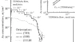
Local Structure and Anti-Structural Defects of Tin in Amorphous and Crystalline Ge2Sb2Te5 Films A. V. MarchenkoE. I. TerukovP. P. Seregin NONELECTRONIC PROPERTIES OF SEMICONDUCTORS (ATOMIC STRUCTURE, DIFFUSION) 03 February 2021 Pages: 1 - 6
Arsenic Doping Upon the Deposition of CdTe Layers from Dimethylcadmium and Diisopropyltellurium V. S. EvstigneevA. V. ChilyasovD. I. Kuritsyn ELECTRONIC PROPERTIES OF SEMICONDUCTORS 03 February 2021 Pages: 7 - 13
Room-Temperature Observation of Local and Nonlocal Electronic Quantum States on the Surface of Silicon N. A. Torkhov SURFACES, INTERFACES, AND THIN FILMS 03 February 2021 Pages: 14 - 20
Silicon Ultrathin Oxide (4.2 nm)–Polysilicon Structures Resistant to Field Damages D. A. BelorusovE. I. GoldmanG. V. Chucheva SURFACES, INTERFACES, AND THIN FILMS 03 February 2021 Pages: 21 - 24
Thin-Film Baroresistors Based on Sm1 – xGdxS Solid Solutions V. V. KaminskyS. M. SolovievS. E. Alexandrov SURFACES, INTERFACES, AND THIN FILMS 03 February 2021 Pages: 25 - 27
Effect of Annealing on the Surface Morphology and Current–Voltage Characterization of a CZO Structure Prepared by RF Magnetron Sputtering B. KınacıE. ÇelikS. Özçelik SURFACES, INTERFACES, AND THIN FILMS 03 February 2021 Pages: 28 - 36
Spray Pyrolysis Synthesized and ZnO–NiO Nanostructured Thin Films Analysis with Their Nanocomposites for Waveguiding Applications B. GharbiA. TaaboucheB. Rahal SURFACES, INTERFACES, AND THIN FILMS 03 February 2021 Pages: 37 - 43
Spectroscopic Studies of Integrated GaAs/Si Heterostructures P. V. SeredinD. L. GoloshchapovS. O. Slipchenko SEMICONDUCTOR STRUCTURES, LOW-DIMENSIONAL SYSTEMS, AND QUANTUM PHENOMENA 03 February 2021 Pages: 44 - 50
Frequency Dependent Capacitance and Conductance–Voltage Characteristics of Nitride GaAs Schottky Diode A. ZianeM. AmraniA. Bouraiou SEMICONDUCTOR STRUCTURES, LOW-DIMENSIONAL SYSTEMS, AND QUANTUM PHENOMENA 03 February 2021 Pages: 51 - 55
Simulation of Carrier Trapping in an Embedded Nanowire and Its Effect in the Nano-EBIC Technique A. El HdiyM. Ledra SEMICONDUCTOR STRUCTURES, LOW-DIMENSIONAL SYSTEMS, AND QUANTUM PHENOMENA 03 February 2021 Pages: 56 - 60
Quantum-Confinement Effect in Silicon Nanocrystals during Their Dissolution in Model Biological Fluids M. B. GongalskyU. A. TsurikovaL. A. Osminkina MICROCRYSTALLINE, NANOCRYSTALLINE, POROUS, AND COMPOSITE SEMICONDUCTORS 03 February 2021 Pages: 61 - 65
Study of Undoped Nanocrystalline Diamond Films Grown by Microwave Plasma-Assisted Chemical Vapor Deposition A. L. VikharevS. A. BogdanovS. A. Korolev MICROCRYSTALLINE, NANOCRYSTALLINE, POROUS, AND COMPOSITE SEMICONDUCTORS 03 February 2021 Pages: 66 - 75
Structural and Optical-Phonon Properties of InSb Nanocrystals Synthesized in Si and SiO2 Matrices I. E. TyschenkoR. Zhang MICROCRYSTALLINE, NANOCRYSTALLINE, POROUS, AND COMPOSITE SEMICONDUCTORS 03 February 2021 Pages: 76 - 85
Effect of Electron–Phonon Interaction and γ-Ray Irradiation on the Reverse Currents of Silicon Photodiodes S. V. BulyarskiyA. V. LakalinM. A. Saurov PHYSICS OF SEMICONDUCTOR DEVICES 03 February 2021 Pages: 86 - 91
High-Power Schottky Diodes with a Negative-Differential-Resistance Portion in the I–V Characteristic A. G. TandoevT. T. MnatsakanovS. N. Yurkov PHYSICS OF SEMICONDUCTOR DEVICES 03 February 2021 Pages: 92 - 99
Silicon Nanowire Parameter Extraction Using DFT and Comparative Performance Analysis of SiNWFET and CNTFET Devices B. SinghB. PrasadD. Kumar PHYSICS OF SEMICONDUCTOR DEVICES 03 February 2021 Pages: 100 - 107
Effect of Total Ionizing Dose Damage on 8-Transistor CMOS Star Sensor Performance J. FengY.-D. LiQ. Guo PHYSICS OF SEMICONDUCTOR DEVICES 03 February 2021 Pages: 108 - 115
Device Performance Optimization of Organic Thin-Film Transistors at Short-Channel Lengths Using Vertical Channel Engineering Techniques F. AnaN. Din PHYSICS OF SEMICONDUCTOR DEVICES 03 February 2021 Pages: 116 - 121
Structural and Spectroscopic Studies of Epitaxial GaAs Layers Grown on Compliant Substrates Based on a Superstructure Layer and Protoporous Silicon P. V. SeredinD. L. GoloshchapovHarald Leiste FABRICATION, TREATMENT, AND TESTING OF MATERIALS AND STRUCTURES 03 February 2021 Pages: 122 - 131