
Abstract
This chapter describes the characteristic structural and electrical properties of solid-state materials with emphasis on semiconductors, surfaces and interfaces, junctions, charge carrier transport mechanisms, electrical contacts and devices. An overview of semiconductor growth techniques is also included in this chapter for readers to familiarise with some of the terminologies that describe semiconductor/semiconductor (SS), metal/semiconductor (MS) or metal/insulator/semiconductor (MIS) structures. This chapter also includes a description of the concept of bandgap grading and next-generation solar cells.
Access this chapter
Tax calculation will be finalised at checkout
Purchases are for personal use only
References
J. Singh, Electronic and Optoelectronic Properties of Semiconductor Structures (Cambridge University Press, Cambridge, 2003). https://doi.org/10.1017/CBO9780511805745
I.A. Sukhoivanov, I.V. Guryev, Photonic Crystals (Springer, Berlin, 2009). https://doi.org/10.1007/978-3-642-02646-1
D. Neamen, Semiconductor physics and devices. Mater. Today. 9, 57 (2006). https://doi.org/10.1016/S1369-7021(06)71498-5
I.M. Dharmadasa, Advances in Thin-Film Solar Cells (Pan Stanford, Singapore, 2013)
W.H. Strehlow, E.L. Cook, Compilation of energy band gaps in elemental and binary compound semiconductors and insulators. J. Phys. Chem. Ref. Data. 2, 163–200 (1973). https://doi.org/10.1063/1.3253115
S.M. Sze, K.K. Ng, Physics of Semiconductor Devices (Wiley, Hoboken, 2006). https://doi.org/10.1002/0470068329
A.A. Ojo, I.M. Dharmadasa, 15.3% efficient graded bandgap solar cells fabricated using electroplated CdS and CdTe thin films. Sol. Energy. 136, 10–14 (2016). https://doi.org/10.1016/j.solener.2016.06.067
S.D. Sathaye, A.P.B. Sinha, Studies on thin films of cadmium sulphide prepared by a chemical deposition method. Thin Solid Films 37, 15–23 (1976). https://doi.org/10.1016/0040-6090(76)90531-9
I.M. Dharmadasa, J.M. Thornton, R.H. Williams, Effects of surface treatments on Schottky barrier formation at metal/n-type CdTe contacts. Appl. Phys. Lett. 54, 137 (1989). https://doi.org/10.1063/1.101208
I.M. Dharmadasa, J.D. Bunning, A.P. Samantilleke, T. Shen, Effects of multi-defects at metal/semiconductor interfaces on electrical properties and their influence on stability and lifetime of thin film solar cells. Sol. Energy Mater. Sol. Cells. 86, 373–384 (2005). https://doi.org/10.1016/j.solmat.2004.08.009
T.L. Chu, S.S. Chu, C. Ferekides, J. Britt, C.Q. Wu, Thin-film junctions of cadmium telluride by metalorganic chemical vapor deposition. J. Appl. Phys. 71, 3870–3876 (1992). https://doi.org/10.1063/1.350852
L. Huang, Y. Zhao, D. Cai, Homojunction and heterojunction based on CdTe polycrystalline thin films. Mater. Lett. 63, 2082–2084 (2009). https://doi.org/10.1016/j.matlet.2009.06.028
B.E. McCandless, J.R. Sites, in Handb. Photovolt. Sci. Eng. Cadmium telluride solar cells (Wiley, Chichester, 2011), pp. 600–641. https://doi.org/10.1002/9780470974704.ch14.
M.P. Mikhailova, A.N. Titkov, Type II heterojunctions in the GaInAsSb/GaSb system. Semicond. Sci. Technol. 9, 1279–1295 (1994). https://doi.org/10.1088/0268-1242/9/7/001.
P. Hofmann, Solid State Physics: An Introduction, 2nd edn. (Wiley-VCH, Berlin, 2015)
P.V. Meyers, Advances in CdTe n-i-p photovoltaics. Sol. Cells. 27, 91–98 (1989). https://doi.org/10.1016/0379-6787(89)90019-7
E.H. Rhoderick, The physics of Schottky barriers? Rev. Phys. Technol. 1, 81–95 (1970). https://doi.org/10.1088/0034-6683/1/2/302
W.G. Oldham, A.G. Milnes, n-n Semiconductor heterojunctions. Solid. State. Electron. 6, 121–132 (1963). https://doi.org/10.1016/0038-1101(63)90005-4
E.H. Rhoderick, Metal-semiconductor contacts. IEE Proc. I Solid State Electron Devices. 129, 1 (1982). https://doi.org/10.1049/ip-i-1.1982.0001
J.P. Ponpon, A review of ohmic and rectifying contacts on cadmium telluride. Solid. State. Electron. 28, 689–706 (1985). https://doi.org/10.1016/0038-1101(85)90019-X
I.M. Dharmadasa, Recent developments and progress on electrical contacts to CdTe, CdS and ZnSe with special reference to barrier contacts to CdTe. Prog. Cryst. Growth Charact. Mater. 36, 249–290 (1998). https://doi.org/10.1016/S0960-8974(98)00010-2
J. Bardeen, Surface states and rectification at a metal semi-conductor contact. Phys. Rev. 71, 717–727 (1947). https://doi.org/10.1103/PhysRev.71.717
J. Singh, Semiconductor Devices: Basic Principles (Wiley, New York, 2001)
W.E. Spicer, I. Lindau, P. Skeath, C.Y. Su, P. Chye, Unified mechanism for Schottky-barrier formation and III-V oxide interface states. Phys. Rev. Lett. 44, 420–423 (1980). https://doi.org/10.1103/PhysRevLett.44.420
R. Schlaf, R. Hinogami, M. Fujitani, S. Yae, Y. Nakato, Fermi level pinning on HF etched silicon surfaces investigated by photoelectron spectroscopy. J. Vac. Sci. Technol. A 17, 164 (1999). https://doi.org/10.1116/1.581568
I.M. Dharmadasa, O. Elsherif, G.J. Tolan, Solar cells active in complete darkness. J. Phys. Conf. Ser. 286, 12041 (2011). https://doi.org/10.1088/1742-6596/286/1/012041
H.J. Queisser, Defects in semiconductors: some fatal, some vital. Science 281, 945–950 (1998). https://doi.org/10.1126/science.281.5379.945
R.B. Godfrey, M.A. Green, Enhancement of MIS solar-cell “efficiency” by peripheral collection. Appl. Phys. Lett. 31, 705–707 (1977). https://doi.org/10.1063/1.89487
W.A. Nevin, G.A. Chamberlain, Effect of oxide thickness on the properties of metal-insulator-organic semiconductor photovoltaic cells. IEEE Trans. Electron Devices. 40, 75–81 (1993). https://doi.org/10.1109/16.249427
M.A. Green, Solar cell efficiency tables (version 49). Prog. Photovolt. Res. Appl. 25, 3–13 (2017). https://doi.org/10.1002/pip.2876
V.M. Fthenakis, Life cycle impact analysis of cadmium in CdTe PV production. Renew. Sustain. Energy Rev. 8, 303–334 (2004). https://doi.org/10.1016/j.rser.2003.12.001
B.M. Basol, High-efficiency electroplated heterojunction solar cell. J. Appl. Phys. 55, 601–603 (1984). https://doi.org/10.1063/1.333073
J. Nelson, Polymer:fullerene bulk heterojunction solar cells. Mater. Today. 14, 462–470 (2011). https://doi.org/10.1016/S1369-7021(11)70210-3
J. Nelson, Organic photovoltaic films. Curr. Opin. Solid State Mater. Sci. 6, 87–95 (2002). https://doi.org/10.1016/S1359-0286(02)00006-2
S. Gunes, N.S. Sariciftci, Hybrid solar cells. Inorganica Chim. Acta. 361, 581–588 (2008). https://doi.org/10.1016/j.ica.2007.06.042
M. Wright, A. Uddin, Organic-inorganic hybrid solar cells: a comparative review. Sol. Energy Mater. Sol. Cells. 107, 87–111 (2012). https://doi.org/10.1016/j.solmat.2012.07.006
W. Xu, F. Tan, X. Liu, W. Zhang, S. Qu, Z. Wang, Z. Wang, Efficient organic/inorganic hybrid solar cell integrating polymer nanowires and inorganic nanotetrapods. Nanoscale Res. Lett. 12, 11 (2017). https://doi.org/10.1186/s11671-016-1795-9
P.-L. Ong, I.A. Levitsky, Organic/IV, III-V semiconductor hybrid solar cells. Energies. 3, 313–334 (2010). https://doi.org/10.3390/en3030313
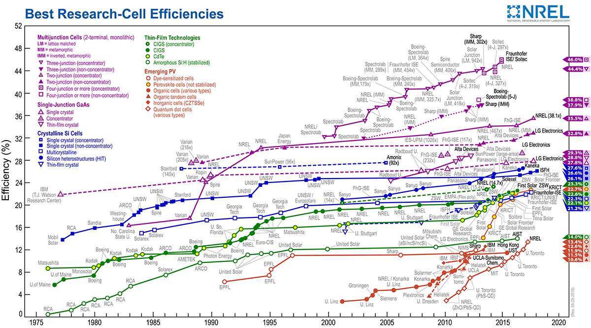
NREL efficiency chart. (n.d.), https://www.nrel.gov/pv/assets/images/efficiency-chart.png. Accessed 19 June 2017
I.M. Dharmadasa, Third generation multi-layer tandem solar cells for achieving high conversion efficiencies. Sol. Energy Mater. Sol. Cells. 85, 293–300 (2005). https://doi.org/10.1016/j.solmat.2004.08.008
O. Ergen, S.M. Gilbert, T. Pham, S.J. Turner, M.T.Z. Tan, M.A. Worsley, A. Zettl, Graded bandgap perovskite solar cells. Nat. Mater. 16, 522–525 (2016). https://doi.org/10.1038/nmat4795
I.M. Dharmadasa, A.A. Ojo, H.I. Salim, R. Dharmadasa, Next generation solar cells based on graded bandgap device structures utilising rod-type nano-materials. Energies. 8, 5440–5458 (2015). https://doi.org/10.3390/en8065440
J. Tauc, Generation of an emf in semiconductors with nonequilibrium current carrier concentrations. Rev. Mod. Phys. 29, 308–324 (1957). https://doi.org/10.1103/RevModPhys.29.308
M. Wolf, Limitations and possibilities for improvement of photovoltaic solar energy converters: part I: considerations for earth’s surface operation. Proc. IRE. 48, 1246–1263 (1960). https://doi.org/10.1109/JRPROC.1960.287647
P.R. Emtage, Electrical conduction and the photovoltaic effect in semiconductors with position-dependent band gaps. J. Appl. Phys. 33, 1950–1960 (1962). https://doi.org/10.1063/1.1728874
M. Konagai, K. Takahashi, Graded-band-gap pGa1-xAlxAs-nGaAs heterojunction solar cells. J. Appl. Phys. 46, 3542–3546 (1975). https://doi.org/10.1063/1.322083
H.J. Hovel, J.M. Woodall, Ga[sub 1−x]Al[sub x]As-GaAs P-P-N heterojunction solar cells. J. Electrochem. Soc. 120, 1246 (1973). https://doi.org/10.1149/1.2403671
I.M. Dharmadasa, A.P. Samantilleke, N.B. Chaure, J. Young, New ways of developing glass/conducting glass/CdS/CdTe/metal thin-film solar cells based on a new model. Semicond. Sci. Technol. 17, 1238–1248 (2002). https://doi.org/10.1088/0268-1242/17/12/306
I. Dharmadasa, J. Roberts, G. Hill, Third generation multi-layer graded band gap solar cells for achieving high conversion efficiencies—II: experimental results. Sol. Energy Mater. Sol. Cells. 88, 413–422 (2005). https://doi.org/10.1016/j.solmat.2005.05.008
A.S. Brown, M.A. Green, Impurity photovoltaic effect: fundamental energy conversion efficiency limits. J. Appl. Phys. 92, 1329–1336 (2002). https://doi.org/10.1063/1.1492016
K.W.J. Barnham, G. Duggan, A new approach to high-efficiency multi-band-gap solar cells. J. Appl. Phys. 67, 3490–3493 (1990). https://doi.org/10.1063/1.345339
T. Trupke, M.A. Green, P. Würfel, Improving solar cell efficiencies by down-conversion of high-energy photons. J. Appl. Phys. 92, 1668 (2002)
Y.Y. Lee, W.J. Ho, Y.T. Chen, Performance of plasmonic silicon solar cells using indium nanoparticles deposited on a patterned TiO2 matrix. Thin Solid Films. 570, 194–199 (2014). https://doi.org/10.1016/j.tsf.2014.05.022
Y. Takeda, T. Motohiro, Highly efficient solar cells using hot carriers generated by two-step excitation. Sol. Energy Mater. Sol. Cells. 95, 2638–2644 (2011). https://doi.org/10.1016/j.solmat.2011.05.023
J.F. Geisz, D.J. Friedman, J.S. Ward, A. Duda, W.J. Olavarria, T.E. Moriarty, J.T. Kiehl, M.J. Romero, A.G. Norman, K.M. Jones, 40.8% efficient inverted triple-junction solar cell with two independently metamorphic junctions. Appl. Phys. Lett. 93, 123505 (2008). https://doi.org/10.1063/1.2988497
A.B.F. Martinson, M.S. Góes, F. Fabregat-Santiago, J. Bisquert, M.J. Pellin, J.T. Hupp, Electron transport in dye-sensitized solar cells based on ZnO nanotubes: evidence for highly efficient charge collection and exceptionally rapid dynamics. J. Phys. Chem. A. 113, 4015–4021 (2009). https://doi.org/10.1021/jp810406q
T. Stelzner, M. Pietsch, G. Andrä, F. Falk, E. Ose, S. Christiansen, Silicon nanowire-based solar cells. Nanotechnology. 19, 295203 (2008). http://stacks.iop.org/0957-4484/19/i=29/a=295203
F.V. Wald, Applications of CdTe. A review. Rev. Phys. Appliquée. 12, 277–290 (1977). https://doi.org/10.1051/rphysap:01977001202027700
R. Frerichs, The photo-conductivity of “incomplete phosphors”. Phys. Rev. 72, 594–601 (1947). https://doi.org/10.1103/PhysRev.72.594
J.J. Loferski, Theoretical considerations governing the choice of the optimum semiconductor for photovoltaic solar energy conversion. J. Appl. Phys. 27, 777–784 (1956). https://doi.org/10.1063/1.1722483
A. Luque, S. Hegedus, Handbook of Photovoltaic Science and Engineering (Wiley, Chichester, 2010). https://doi.org/10.1002/9780470974704
Author information
Authors and Affiliations
Rights and permissions
Copyright information
© 2019 Springer International Publishing AG, part of Springer Nature
About this chapter

Cite this chapter
Ojo, A.A., Cranton, W.M., Dharmadasa, I.M. (2019). Photovoltaic Solar Cells: Materials, Concepts and Devices. In: Next Generation Multilayer Graded Bandgap Solar Cells. Springer, Cham. https://doi.org/10.1007/978-3-319-96667-0_2
Download citation
DOI: https://doi.org/10.1007/978-3-319-96667-0_2
Published:
Publisher Name: Springer, Cham
Print ISBN: 978-3-319-96666-3
Online ISBN: 978-3-319-96667-0
eBook Packages: EnergyEnergy (R0)