
Abstract
For nearly a century, rectifier circuits have been the most common power electronic circuits used to convert ac to dc. The word rectification is used not because these circuits produce dc but rather because the current flows in one direction; only the average output signal (voltage or current) has a dc component. Moreover, since these circuits allow power to flow only from the source to the load, they are often termed unidirectional converters. As will be shown shortly, when rectifier circuits are used solely, their outputs consist of dc along with high-ripple ac components. To significantly reduce or eliminate the output ripple, additional filtering circuitry is added at the output. In the majority of applications, diode rectifier circuits are placed at the front end of the power electronic 60 Hz systems, interfaced with the sine-wave voltage produced by the electric utility. In dc-dc application, at the rectified side or the dc side, a large filter capacitor is added to reduce the rectified voltage ripple. This dc voltage maintained across the output capacitor is known as raw dc or uncontrolled dc.
Author information
Authors and Affiliations
Problems
Problems
In all the problems assume ideal diodes unless stated otherwise.
7.1.1 Single-Phase Rectifiers
7.1.1.1 Half-Wave Rectifiers
-
7.1
Determine the power factor and the THD for the waveforms of Example 7.1.
-
7.2
Consider the half-wave rectifier in Fig. P7.2 with v s = 110 sin ωt V and R = 1 kΩ. Assume ideal diode except the forward resistance (r d) is 10 Ω. Sketch v o and determine (a) the average output voltage, (b) the rms current in the diode, (c) the peak current in the diode, and (d) the input power factor.
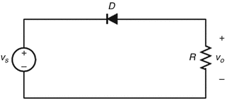
Fig. P7.2
- 7.3
-
7.4
Consider the half-wave inductive-load rectifier circuit of Fig. 7.4a with \( {v}_{\mathrm{s}}=110\sqrt{2}\sin \omega t\kern0.5em \mathrm{V} \), ω = 60 Hz, L = 800 mH, and R = 100 Ω. Find (a) the expression for i L(t), (b) the time t 1 when i L becomes zero, (c) the average load current, (d) the peak inductor current, (e) the rms current in the inductor, and (f) the average power delivered to the load.
-
7.5
Repeat Problem 7.4 with the diode reversed.
-
7.6
Repeat Problem 7.4 by placing a free-wheeling diode in parallel with the load as shown in Fig. 7.6a.
- 7.7
-
D7.8
Design for L and R for the half-wave rectifier of Fig. 7.6a to provide a ripple current not to exceed 5% of its average value at V o = 20 V. Assume v s = 40 sin 120ωt V.
-
D7.9
The single-phase, half-wave rectifier of Fig. 7.6a is required to supply the load with an output ripple current not to exceed 5% of its dc value. (a) Design for L to meet this requirement. Use R = 20 Ω, v s = 150 sin 120πt V, (b) what is the average load voltage.
-
7.10
Derive Eqs. (7.20) and (7.21) for the half-wave rectifier with an L − R load.
-
D7.11
Design a half-wave rectifier of Fig. 7.4a with an L − R load to supply 25 W to the load with a minimum output ripple current of 10% and an average output of 85 V. Use v s = 120 sin(120πt) .
-
D7.12
Design a dc power supply with an average dc output of 20 V with a 2% ripple. The power supply should be capable of providing 500 mA to the load. Use the rectifier of Fig. P7.12 for your design with v s = 110 sin(2π60t) V and assume the diode’s forward voltage drop is 1V. Specify the diode’s ratings including its peak reverse voltage and rms values.
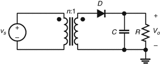
Fig. P7.12
-
D7.13
Design the half-wave rectifier with an R-C load with a 10% output ripple voltage and which provides 10 W to the load. Assume v s = 20 sin(120πt)V.
-
7.14
Sketch the waveforms for i s, i c, i R, and v o for Fig. 7.8a with R = 10 kΩ, C = 100μF, and v s = 10 sin(377πt)V.


7.1.1.2 Full-Wave Rectifiers
-
7.15
Determine the power factor and the THD for the waveforms of Fig. 7.3b.
-
7.16
Consider the full-wave rectifier with a resistive load of Fig. 7.3a with v s = 120 sin ωt and R = 20 Ω. Find: (a) the average output voltage, (b) the average output current, (c) the rms output current, (d) the input power factor, and (e) the load power.
-
7.17
Consider a full-wave rectifier with an infinite inductive load.
-
(a)
Show that the dc and harmonic components of the output voltage are given by:
For n = 2, 4, 6, …
-
(b)
Show that the nth harmonics of the source current is given below:
-
D7.18
It is required that the circuit shown in Fig. P7.18 provides an output power of 2 kW at an average load current of 20 A. Design for the transformer turns ratio and R to meet this requirement. Assume L/R ≫ T. Use v s = 100 sin(2π60t) V.
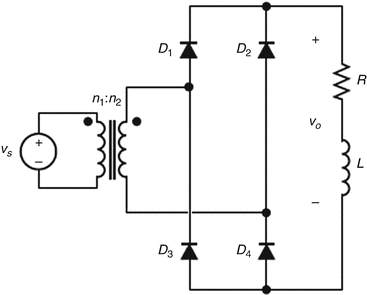
Fig. P7.18
-
7.19
Consider the generalized-type load with a dc source representing a dc motor load full-wave rectifier as shown in Fig. P7.19. Assume v s = V s sin ωt V and V DC < V s. Derive (a) the expression for i o(t), (b) the rms value of i o(t), (c) the average load current, and (d) the ripple load current and (e) calculate the above values for V s = 25 V, ω = 377 rad/s, R = 2 Ω, and L = 5 mH.
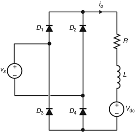
Fig. P7.19
-
7.20
Consider the center-tap full-wave rectifier of Fig. P7.20. (a) Sketch v o, (b) determine V o, (c) repeat parts (a) and (b) by including each diode drop V D, and (d) determine the peak inverse voltage (PIV) for the two diodes.
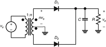
Fig. P7.20
-
D7.21
If it is required to design the full-wave rectifier of Problem 7.20 to provide an average output voltage of 48 V with an output power of 25 W. Design for the required transformer turns ratio n. Assume\( {v}_{\mathrm{s}}=110\sqrt{2}\sin 377t\ \mathrm{V} \).
-
D7.22
Redesign Problem 7.21 by assuming V s(t) fluctuates by±20%. Design for the worst case.
-
7.23
Consider the full-wave center-tap diode rectifier circuit shown in Fig. P7.23. (a) Sketch v o1 and v o2 and (b) determine the peak inverse voltage for each diode.
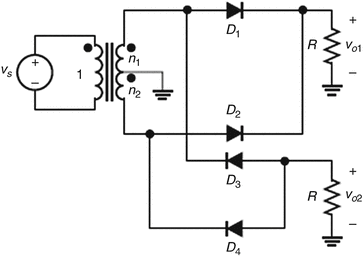
Fig. P7.23
-
D7.24
Design the dual center-tap full-wave rectifier of Fig. P7.24 to provide ±15 V dc from a line voltage v s = 155 sin ωt V, where ω = 377 rad/s.
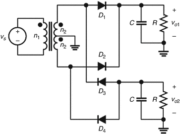
Fig. P7.24
-
7.25
Repeat Problem 7.9 by using the full-bridge rectifier given in Fig. 7.20a with L s = 0.
-
7.26
(a) Calculate the output ripple voltage for the full-wave rectifier of Fig. P7.26. Use R = 10 kΩ and C = 47 μF, with v s = 20 sin 120ωt V.
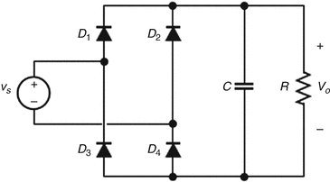
Fig. P7.26
-
(b)
Show that the expression for the average output voltage is given by:


where τ = RC and t 1 (0 < t 1 < T/4) is the time at which the diode starts conducting.
-
(c)
Show that if it is assumed that the ripple voltage is much smaller than the peak input voltage, i.e., t 1 = T/4, and RC ≫ T, then show that V r = V s/2RCf. Apply this simplified ripple voltage to part (a).
-
(d)
Use the approximation in part (c) to show that the average diode current is given by:
-
7.27
The circuit shown in Fig. P7.27 is called a voltage doubler. It is used when the line voltage of a given system changes from 110 VAC to 220 VAC or vice versa. By changing the switch position, the output voltage can be held constant under both a 110 VAC and a 220 VAC line inputs. Consider the following voltage doubler. (a) Determine the voltages v o1 and v o2 for both cases when the switch is on and off. Assume v s = V s sin ωt V with R 1 C 1 ≫ T and R 2 C 2 ≫ T.
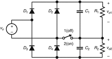
Fig. P7.27
-
7.28
Consider the full-wave rectifier with an LC output filter shown in Fig. P7.28. (a) Draw the equivalent circuit seen between a and b by assuming L = 0 an C = ∞d, (b) repeat part (a) by assuming L = ∞ and C = 0, and (c) calculate the power dissipated in the load in parts (a) and (b). Assume v s = V s sin ωt.
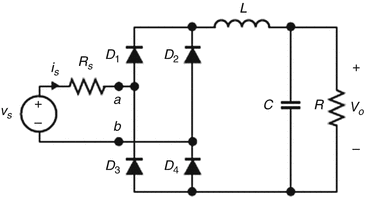
Fig. P7.28
-
7.29
The single-phase, full-wave rectifier with an R-C load shown in Fig. P7.26. (a) is required to supply the load with an output ripple voltage not to exceed 5% of its dc value. (a) Design for C to meet this requirement. Use R = 20 Ω, v s = 150 sin 120ωt V and (b) calculate the average load current.


7.1.2 The Effect of ac-Side Inductance
7.1.2.1 Half-Wave Circuits
-
7.30
Consider the half-wave rectifier shown in Fig. P7.30 with a flyback diode including L s and the diode resistances. Assume v s = V s sin ωt V. (a) Derive the expression for the power dissipated in the rectifier. (b) Sketch i s, i D2, and v o .
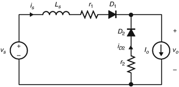
Fig. P7.30
-
7.31
It is required to design the circuit of Fig. 7.12a to deliver a 1kW output power at I o = 20 A. Assume L s fluctuates in the range of ± 20%. Use L s = 0.1 mH and v s(t) = 120 sin 2π60t V. Design for the load resistance and inductance.

7.1.2.2 Full-Wave Circuits
-
7.32
Derive the rms and fundamental component expressions for the input current i s(t) of a full-wave rectifier circuit with an ac-side inductance which is redrawn in Fig. P7.32.
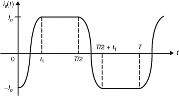
Fig. P7.32
-
7.33
Repeat Problem 7.32 by the approximation for i s(t) as shown in Fig. P7.33.

Fig. P7.33
-
7.34
(a) Discuss the operations of the circuit in Fig. P7.34 and sketch the waveforms for v o, i s1, i s2, v Ls1, v Ls2. Assume v s1 = V s1 sin ωt V, v s2 = V s2 sin ωt V. (b) Derive the expression for v o(t). (c) What is the difference between this circuit and the full-wave bridge circuit of Fig. 7.21?
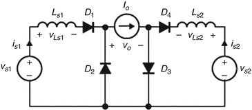
Fig. P7.34
-
7.35
(a) Find the ratio between the rms currents for the waveforms shown in Fig. P7.35a, b representing the line current for half-wave rectifiers with and without an ac-side inductance, respectively. (b) Sketch the ratios as a function of ωt 1 = u.
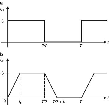
Fig. P7.35


7.1.2.3 Input Power Factor
-
7.36
Consider the line current for the half-wave rectifier with L s as shown in Fig. 7.12e, which is redrawn in Fig. P7.36a. (a) Derive the expression for the power factor for i s(t), (b) repeat part (a) by using the trapezoidal approximation as shown in Fig. P7.36b, c compare the two solutions.
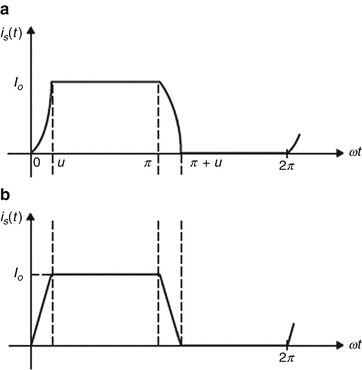
Fig. P7.36
-
7.37
Consider the one-port converter network shown in Fig. P7.37 with i s = 5 sin(377t + 30°) A, and v s = 10 sin(377t − 45°) V. Determine (a) the instantaneous input power, (b) the input power factor, and (c) the average input power.
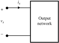
Fig. P7.37
-
7.38
Derive the input power factor and the THD for the input current waveforms shown in Fig. P7.38. Assume the line voltage is pure sinusoidal.
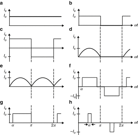
Fig. P7.38


7.1.2.4 Three-Phase Rectifier Circuit
-
7.39
(a) Show that the average output voltage for the n-phase, half-wave rectifier of Fig. P7.39 is given by:
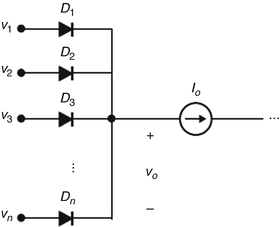
Fig. P7.39

where V s is the phase peak voltage. What is the value of V o as n → ∞\( ? \)
-
(b)
Show that the rms and average current in each diode is given by:
-
7.40
Consider the balanced three-phase rectifier circuit shown in Fig. P7.40 with the delta-connected voltage sources given below:
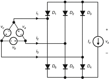
Fig. P7.40

(a) Sketch the waveform for i 1, i 2, i 3, v o , (b) derive the expression for the average V o, and (c) determine the first fundamental component for the line current.
-
7.41
Consider the half-wave three-phase capacitive load circuit of Fig. P7.41. (a) Determine the rms value for v o, (b) calculate the input power factor for each phase, and (c) sketch v o for RC = T/3.
Fig. P7.41

7.1.2.5 Three-Phase Rectifiers with ac-Side Inductance
-
7.42
Derive Eq. (7.60) for the average output voltage for the half-wave, three-phase converter.
-
7.43
Design the transformer turns ratio of the circuit shown in Fig. P7.43 to deliver a 10 A load current with a 120 V output voltage. Assume the line-to-line voltages are 580 VAC, with ω = 2π60 and L s = 1 mH.
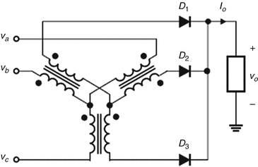
Fig. P7.43
-
7.44
Derive Eq. (7.64) for the commutation angle u for the full-wave converter.

7.1.2.6 General Problem
-
7.45
Sketch the input current, i s, and output voltage, v o, for the circuit shown in Fig. P7.45.
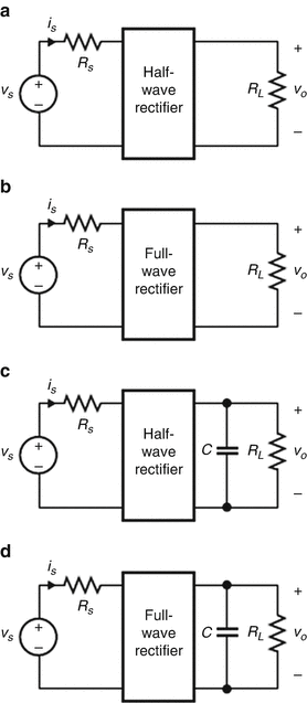
Fig. P7.45

Assume v s(t) = V s sin ωt V.
-
7.46
Derive the expression for the average output power and the commutation angle u for the circuit shown in Fig. P7.46. Find the average and rms values of each diode current. Assume v s(t) = V s sin ωt V.
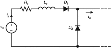
Fig. P7.46
-
7.47
In problem 7.46, if we assume that D 1 and D 2 have forward resistances r D1 and r D2, respectively, show that the commutation angle is given by

-
7.48
Find the average output voltage for the circuit of Fig. P7.48. Determine the percentage change in the average output voltage if the ac-side line inductance doubles. Assume \( {v}_{\mathrm{s}}=110\sqrt{2}\sin 377t\ \mathrm{V} \).
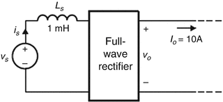
Fig. P7.48
-
7.49
Consider the full-wave rectifier with an ac-side line inductance and a dc-source in the load side as shown in Fig. P7.49. (a) Sketch i o, i s, and v Ls, (b) calculate the average output power, and (c) calculate the percentage change in the average output power if the ac-side line inductance doubles in value. Assume v s = 50 sin 2π60t V.
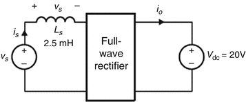
Fig. P7.49
-
7.50
Repeat Problem 7.49 for v s being a square wave with ±50 V peaks and T = 20 ms.
-
7.51
Sketch the waveforms for i s1, i s2, and \( {v}_{\mathrm{s}}^{\prime } \) for the circuit in Fig. P7.51. Find the THD for\( {v}_{\mathrm{s}}^{\prime } \).
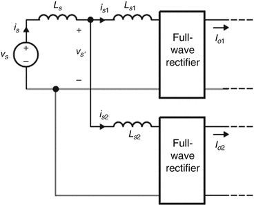
Fig. P7.51
-
7.52
Derive the expression for the average output voltage in Fig. P7.52 in terms of the circuit parameters, assuming v s(t) = V s sin ωt.
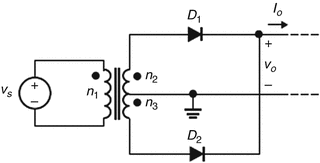
Fig. P7.52
-
7.53
Repeat problem 7.52 by assuming that there exist an ac-side line inductance and diode resistors r D1 and r D2 as shown in Fig. P7.53.
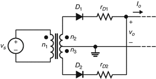
Fig. P7.53


Rights and permissions
Copyright information
© 2018 Springer International Publishing AG
About this chapter

Cite this chapter
Batarseh, I., Harb, A. (2018). Uncontrolled Diode Rectifier Circuits. In: Power Electronics. Springer, Cham. https://doi.org/10.1007/978-3-319-68366-9_7
Download citation
DOI: https://doi.org/10.1007/978-3-319-68366-9_7
Published:
Publisher Name: Springer, Cham
Print ISBN: 978-3-319-68365-2
Online ISBN: 978-3-319-68366-9
eBook Packages: EngineeringEngineering (R0)