
Abstract
In this chapter, several general concepts will be discussed to provide necessary background material in power electronics. The review material will cover switching diode circuits, power computation, harmonic analysis, and component concepts.
Notes
- 1.
Also known as the homogeneous solution.
- 2.
This Q has nothing to do with resonant circuit parameter Q discussed earlier and the one to be discussed in Chap. 6.
- 3.
It is also common to represent a n and b n in terms of frequency as follows:
$$ {a}_n=\frac{1}{\uppi}{\int}_0^{2\uppi}f\left(\upomega \mathrm{t}\right)\kern.2em \sin \left(n\upomega \mathrm{t}\right)\kern.2em d\left(\upomega \mathrm{t}\right)\kern0.5em {b}_{\mathrm{n}}=\frac{1}{\uppi}{\int}_0^{2\uppi}f\left(\upomega \mathrm{t}\right)\kern.2em \cos \left(n\upomega \mathrm{t}\right)\kern.2em d\left(\upomega t\right)\kern.5em \mathrm{and}\kern.5em {F}_0=\frac{1}{2\uppi}{\int}_0^{2\uppi}f\left(\upomega t\right)d\left(\upomega t\right) $$
Author information
Authors and Affiliations
Problems
Problems
In all the problems, assume ideal diodes unless stated otherwise.
-
3.1
Derive the expressions for i L(t) and v c(t) in switching circuits shown in Fig. P3.1. Assume all initial conditions are zero. Use V dc = 20 V, I dc = 2 A, R = 200 Ω, C = 0.01 μF, and L = 2 mH, sketch i L and v C.
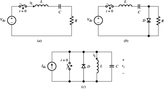
Fig. P3.1
-
3.2
Assume the switch in Fig. P3.2 is opened at t = 0+, derive the expressions for i L, v c and i sw and sketch them for t > 0. Assume i L(0) = I g and v c(0) = V o.
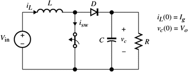
Fig. P3.2
-
3.3
Consider the switching diode circuits of Fig. P3.3 for t > 0 when the switch is turned on. (a) Derive expressions for i L(t), i sw(t), and v c(t). Assume i L(0) = 1.0I g and v c(0) = V o. Suggest possible switch implementations (unidirectional or bidirectional).
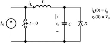
Fig. P3.3
-
3.4
Consider the transistor switching circuits of Fig. P3.4. At t = 0 the transistor is turned on by a signal to the base. Derive and sketch the waveforms for i Q , i L , v c , and v o . Assume v c (0) = −20 V and i L (0) = 0. Compare the two circuits.
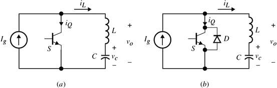
Fig. P3.4
-
3.5
Consider the diode circuit of Fig. P3.5 with switch S 1 opened and S 2 closed at t = 0. Assume the initial conditions are given as v c1(0) = 0 and i L(0) = − 0.5 I g . Derive the expressions for v c1 and i L and sketch them. Use I g = 2 A, C 1 = C 2 = 0.01 μF, and L = 2 mH.
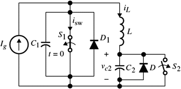
Fig. P3.5
-
3.6
Assume the switch in Fig. P3.6 is opened at t = 0+. Derive the expressions and sketch the waveforms for v c1, v c2, i L, and i D. Assume v c1(0) = v c2(0) and i L(0) = 0.
Fig. P3.6
-
3.7
Consider the capacitor current shown in Fig. P3.7 for a given switch-mode power supply with C = 1 μF, and assume v c (0) = 100 V. (a) Sketch v C showing the peak values and times, and (b) determine the ripple voltage across the capacitor.
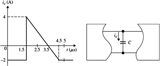
Fig. P3.7
-
3.8
Consider the SCR-diode switching circuit shown in Fig. P3.8 with the switch closing at t = 0. This circuit is a voltage-commutation circuit known as the impulse-commuted chopper used to force the turnoff of the SCR by additional switch S. Assume ideal diode and the capacitor were initially charged to−V o and the SCR was on for t < 0.
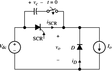
Fig. P3.8
-
(a)
Sketch the waveforms of i SCR, v c, i D, and v o.
-
(b)
Show that the time, Δt, it takes for i C to reach zero again after t > 0 is given by:
$$ \Delta t=\frac{\left({V}_{dc}+{V}_o\right)C}{I_o} $$
Discuss the drawback of such an arrangement.
-
(a)
-
3.9
For the SCR to turn off in the circuit of Fig. P3.8, the capacitor voltage must first be charged to a large negative value. This is done through an external circuit consisting of a diode and an inductance as shown in Fig. P3.9. The purpose of D 1 and L is that when the switch is turned off, the capacitor voltage returns to its original negative value, −V o. Assume S and SCR were open for a long time with a capacitor initial value equal to+V o. At t = 0, SCR is triggered. Sketch the waveforms for i D1, i D0, i SCR, v C, and v o. Compare this circuit with the circuit given in Problem 3.8.
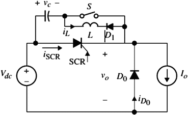
Fig. P3.9
-
3.10
Consider the SCR circuit shown in Fig. P3.10. Because the SCR turns OFF naturally due to the fact that its current becomes zero, the circuit is known as a self-commutated circuit. At t = 0, the SCR is turned ON by applying i g . Derive the expressions for v c(t), i L(t), and the SCR commutation time. Let L = 0.1 mH, C = 47 μF, and V dc = 120 V. Assume the initial capacitor voltage is (i) zero and (ii) −V i (where |V i| < V dc ).
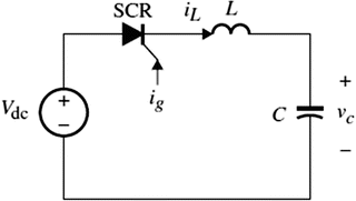
Fig. P3.10
-
D3.11
Design for L and C in Problem 3.10 so that the SCR commutation time is 100 μs, and the peak capacitor voltage does not exceed 200 V.
-
3.12
Consider a source terminal connected to a power electronic circuit whose current and voltage waveforms are shown in Fig. P3.12, with t 1 = 4 μs and T = 10 μs.
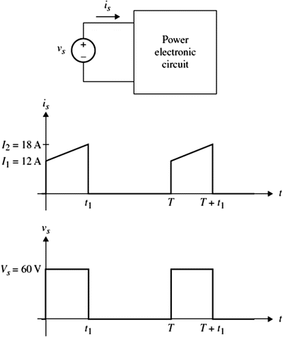
Fig. P3.12
-
(a)
Calculate the average and rms source current and source voltage values.
-
(b)
Calculate the average input power.
-
(a)
-
3.13
Consider the circuit of Fig. P3.13 where v s is a train of pulses as shown. Assume RC ≫ T so that V o is assumed constant and equal to 75 V. Sketch the steady-state inductor current waveform, i L.
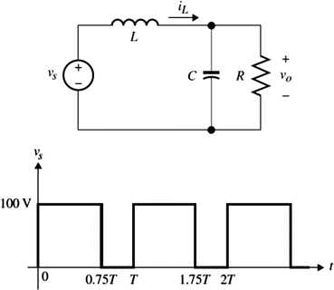
Fig. P3.13
-
3.14
The switch in Fig. P3.14 is closed at t = 0. Assume ideal diodes and all inductor initial conditions are zero. Obtain the expressions for the inductor current and sketch them for 0 ≤ t ≤ 2T. Assume v s(t) is sinusoidal with ω = 377 rad/s and V s = 100 V. Let L = 1 mH, R = 1 Ω, and V dc = 20 V.
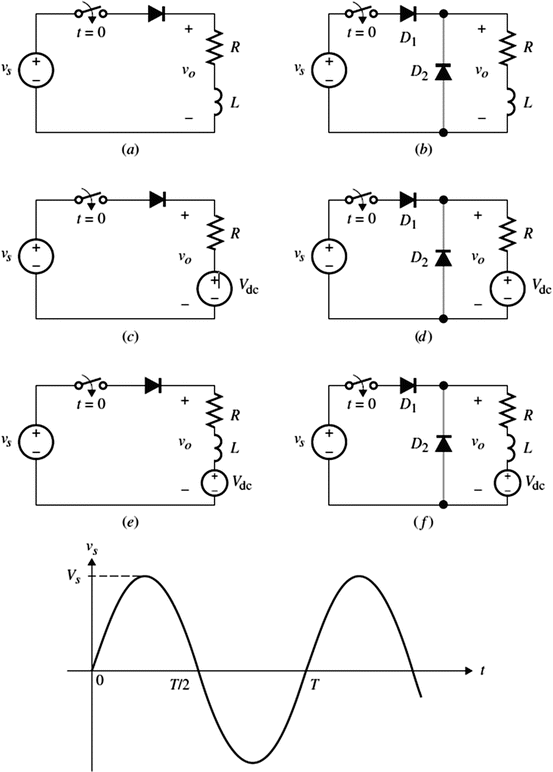
Fig. P3.14
-
3.15
Consider a power source with its terminal voltage and current given as:
$$ {v}_s(t)=100+80\mathit{\sin}\left(\omega t-{100}^{{}^{\circ}}\right)+70\mathit{\cos}\left(2\omega t+{120}^{{}^{\circ}}\right)+25\mathit{\sin}3\omega t\kern0.5em \mathrm{V} $$$$ {i}_s(t)=12+10\mathit{\sin}\left(\omega t+{25}^{{}^{\circ}}\right)+5\mathit{\sin}\left(2\omega t-{30}^{{}^{\circ}}\right)+2\mathit{\cos}3\omega t\kern0.5em \mathrm{A} $$where ω is the fundamental angular frequency.
Calculate:
-
(a)
The rms value of i s(t) and v s(t)
-
(b)
The average input power supplied by the source
-
(c)
The rms values of the fundamental components of i s(t) and v s(t)
-
(d)
THDi and THDv
-
(e)
k dist, k disp, and pf
-
(a)
-
3.16
Consider the phasor circuit of Fig. P3.16 with Z L = 20 ∠ − 36°Ω and V s = 80 ∠ 0° V.
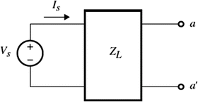
Fig. P3.16
-
(a)
Determine the circuit’s real, apparent, and reactive powers and the input power factor.
-
(b)
Determine the type and value of the load needed to be connected between a and a ′ to achieve unity power factor.
-
(a)
-
3.17
Prove the following integrals:
$$ {F}_n={\int}_0^T\sin n\ \omega t\sin m\ \omega t dt $$$$ ={\int}_0^T\mathit{\cos}n\ \omega t\mathit{\cos}m\ \omega t dt $$$$ =\left\{\begin{array}{c}0\kern3.5em n\ne m\\ {}\frac{T}{2}\kern3.5em n=m\end{array}\right. $$and
$$ {\displaystyle \begin{array}{l}{F}_n={\int}_o^T\sin \left( n\omega t\right)\cos \left( m\omega t\right) dt\\ {}=\left\{\begin{array}{c}0\kern3.75em n\ne m\\ {}-\frac{T}{2}\kern2.75em n=m\end{array}\ \right.\end{array}} $$Where ω = 2π/T, and n = 1, 2, … ∞ ; m = 1, 2, … ∞ .
-
3.18
Sketch the steady-state i L and v L waveforms by assuming the switch in Fig. P3.18 is repeatedly opened and closed as shown. Use T = 10 ms.
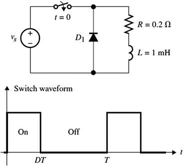
Fig. P3.18
-
3.19
Show that the Fourier series for the half-wave rectifier output voltage of Fig. P3.19 is given by:
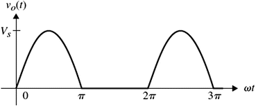
Fig. P3.19
$$ {\boldsymbol{v}}_{\mathbf{o}}\left(\boldsymbol{t}\right)=\frac{{\boldsymbol{V}}_{\mathbf{s}}}{\boldsymbol{\pi}}+\frac{2{\boldsymbol{V}}_{\mathbf{s}}}{\boldsymbol{\pi}}\mathbf{\sin}\boldsymbol{\omega } \boldsymbol{t}-\frac{2{\boldsymbol{V}}_{\mathbf{s}}}{\boldsymbol{\pi}}\sum \limits_{\boldsymbol{n}=2,4,6\dots}^{\infty}\frac{1}{{\boldsymbol{n}}^2-1}\mathbf{\cos}\boldsymbol{\omega } \boldsymbol{t} $$ -
3.20
Show that the Fourier series for the output voltage waveform of a full-wave rectifier of Fig. P3.20 is given by:
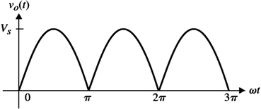
Fig. P3.20
$$ {v}_{\mathrm{o}}(t)=\frac{2{V}_{\mathrm{s}}}{\pi }-\frac{2{V}_{\mathrm{s}}}{\pi}\sum \limits_{n=2,4,6\dots}^{\infty}\frac{1}{n^2-1}\cos \omega t $$ -
3.21
By considering only the first four terms of the Fourier series given in Problem 3.19, verify the answers given in Exercise 3.11.
-
3.22
Derive the Fourier coefficient equations a n and b n given in Eq. (3.41).
-
3.23
The phase current waveform in a three-phase full-wave rectifier SCR circuit under highly inductive load is shown in Fig. P3.23. Show that the harmonics of i(t) are given by the following expression:
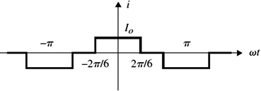
Fig. P3.23
$$ i(t)=\frac{2\sqrt{3}{I}_o}{\pi }\ \left[\mathit{\cos}\omega t-\frac{\mathit{\cos}5\omega t}{5}+\frac{\mathit{\cos}7\omega t}{7}-\frac{\mathit{\cos}11\omega t}{11}+\frac{\mathit{\cos}13\omega t}{13}+\dots \right] $$No triple harmonics in i(t) and n = 6k ± 1(k = 0, 1, 2, …). Show that the rms magnitude of the nth harmonic is\( \sqrt{6}{I}_{\mathrm{o}}/\pi n \).
-
3.24
Show that the Fourier series for the phase current of a six-pulse SCR converter shown in Fig. P3.24 is given by:
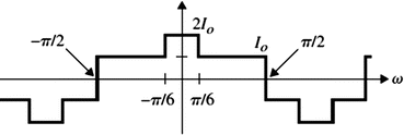
Fig. P3.24
$$ {\displaystyle \begin{array}{l}\boldsymbol{i}\left(\boldsymbol{t}\right)=\frac{6{\boldsymbol{I}}_{\boldsymbol{o}}}{\boldsymbol{\pi}}\left[\boldsymbol{\cos}\boldsymbol{\omega } \boldsymbol{t}+\frac{\boldsymbol{\cos}5\boldsymbol{\omega} \boldsymbol{t}}{5}-\frac{\boldsymbol{\cos}7\boldsymbol{\omega} \boldsymbol{t}}{7}-\frac{\boldsymbol{\cos}11\boldsymbol{\omega} \boldsymbol{t}}{11}+\frac{\boldsymbol{\cos}13\boldsymbol{\omega} \boldsymbol{t}}{13}\right.\\ {}\left.\kern2.3em +\frac{\boldsymbol{\cos}17\boldsymbol{\omega} \boldsymbol{t}}{17}+\dots +\frac{\boldsymbol{\cos}\boldsymbol{n}\boldsymbol{\omega} \boldsymbol{t}}{\boldsymbol{n}}\right]\end{array}} $$ -
3.25
-
(a)
Figure P3.25a shows a typical ac line current waveform in a single-phase, full-wave SCR controlled rectifier circuits under resistance load and sinusoidal ac source. Show that the fundamental line current component is given by:
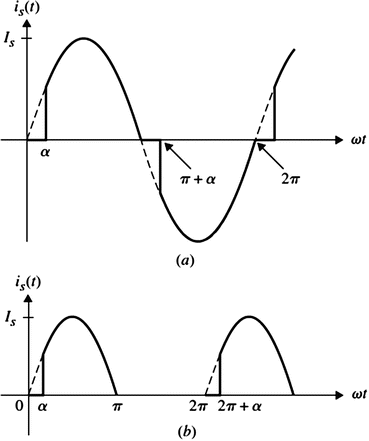
Fig. P3.25
$$ {i}_{\mathrm{s}1}(t)={I}_{\mathrm{s}1}\sin \left(\omega t+\theta \right) $$where
$$ {\displaystyle \begin{array}{l}\omega =\frac{2\pi }{T}\\ {}\theta ={\mathit{\tan}}^{-1}\frac{\mathit{\cos}2\alpha -1}{2\pi -2\alpha +\mathit{\sin}2\alpha}\\ {}{I}_{s1}=\sqrt{1+2{\left(\pi -\alpha \right)}^2+2\left(\pi -\alpha \right)\sin 2\alpha -\cos 2\alpha}\\ {}\kern.5em \times \frac{I_s}{\sqrt{2\pi }}\end{array}} $$ -
(b)
Find i s1(t) for the half-wave SCR controlled line current shown in Fig. P3.25b.
-
(a)
-
3.26
Show that the high harmonic Fourier coefficients for Fig. P3.26 are given by:
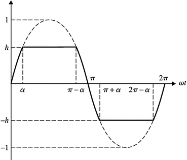
Fig. P3.26
$$ {a}_n=0 $$$$ {b}_n=\frac{1}{\pi}\left(2\alpha +\sin 2\alpha \right)+\sum \limits_{n=3,5,7}^{\infty}\left[\frac{2}{\pi \left(1-n\right)}\sin \alpha \left(1-n\right)\right. $$What value of h will achieve 95% input power factor assuming the waveform represents a line current with a sinusoidal line voltage
-
3.27
Figure P3.27 shows the ac line current for a full-wave, single-phase SCR controlled converter under highly inductive load. Show that the a n coefficients are given by:
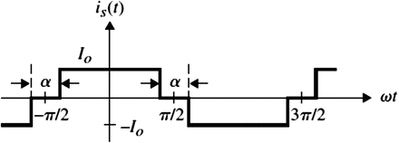
Fig. P3.27
$$ {a}_n=\frac{4{I}_{\mathrm{o}}}{n\pi}\sin \frac{n\left(\pi -\alpha \right)}{2} $$for \( n=1,3,5,7,\dots \)
-
3.28
Show that the Fourier components of i s(t) of Fig. P3.28 are given by:
Fig. P3.28
$$ {i}_{\mathrm{s}}(t)=\frac{4{I}_{\mathrm{o}}}{n\pi}\sum \limits_{n=1,3,5,\dots}^{\infty}\cos n\alpha \sin n\ \omega t $$ -
3.29
Determine the Fourier components for the waveforms given in Fig. P3.29.
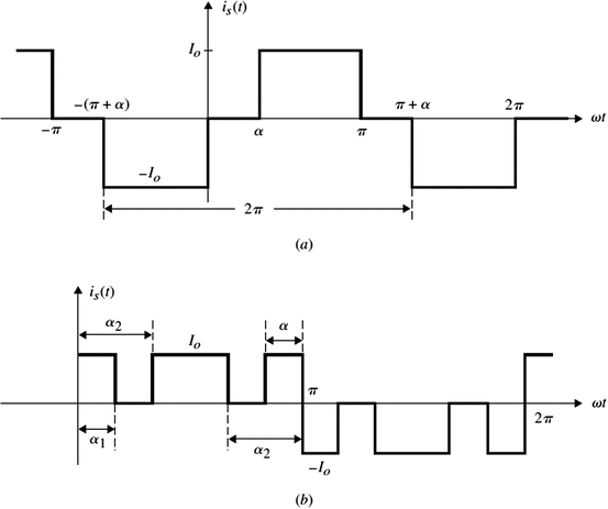
Fig. P3.29


3.1.1 General Problems
-
3.30
In the circuit of Fig. P3.30, the switch is opened at t = 0 after it has been closed for a long time. Derive the expression for i L(t), i D(t) and v C(t) for t > 0, and sketch them.
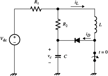
Fig. P3.30
-
3.31
Show that the load current after the switch is closed at t=0 in the diode circuit given in Fig. P3.31 is given by:
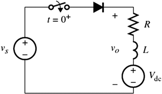
Fig. P3.31
$$ {\displaystyle \begin{array}{cc}\kern8.5em {i}_{\mathrm{o}}(t)=0& 0\le t<{t}_1\\ {}{i}_{\mathrm{o}}(t)=\frac{V_{\mathrm{s}}}{\left|Z\right|}\sin \left(\omega t-\theta \right)-\frac{V_{dc}}{R}+\mathrm{A}{\mathrm{e}}^{-\frac{\mathrm{t}}{\uptau}}& {t}_1\le t<{t}_2\\ {}\kern8.5em {i}_o(t)=0& {t}_2\le t<T\end{array}} $$where
$$ \tau =L/R $$$$ \theta ={\mathit{\tan}}^{-1}\frac{\omega l}{R} $$$$ A=\frac{V_{dc}}{R}-\frac{V_s}{\left|Z\right|}\mathit{\sin}\left(\omega {t}_1-\theta \right) $$Assuming the inductor is not initially charged, and here t 1 is the time when the diode turns on and is given by ωt 1 = sin−1(V dc /V s), and t 2 is the time at which the diode turns off before the next cycle starts at t = T. Find the expression for t 2.
-
3.32
The circuit of Fig. P3.32a is known as a single-phase bridge inverter whose purpose is to convert the dc input voltage, V dc , to an ac output voltage, v o. If the switching sequence of S 1, S 2, S 3, and S 4 is done in such a way that the output voltage is shown in Fig. P3.32b,
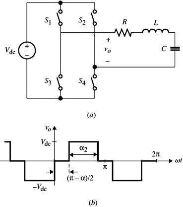
Fig. P3.32
-
(a)
show that the Fourier series for v 0 is given by:
$$ {V}_{\mathrm{o}}={V}_1\sin \omega t+{V}_3\sin 3\ \omega t+{V}_5\sin 5\ \omega t+\dots +{V}_n\sin n\ \omega t $$where
$$ {V}_n=\frac{4{V}_{in}}{n\pi}\mathit{\sin}\frac{n\alpha}{2}\kern3.75em n=1,3,5,7, $$
Use the above results to find the Fourier series for i o(t).
-
(a)
-
3.33
Consider the two-phase switching commutation circuit shown in Fig. P3.33. Assume S 1 has been on for a long time prior to ωt = 150o when S 2 is turned on. (a) Sketch the waveforms for i a(t) and i b(t), and (b) determine the time during which both D 1 and D 2 were on. Assume v a(t) = 100 sin(377t) and v b(t) = 100 sin(377t − 120°) V. Use L S = 1 mH and R s = 2 Ω.
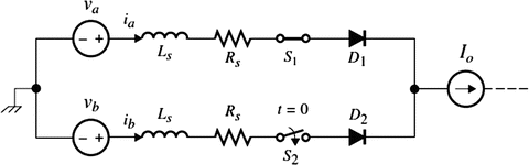
Fig. P3.33
-
3.34
The circuit shown in Fig. P3.34 is known as a forced commutation circuit whose voltage waveform over one switching period, T S, is shown for t > 0. Derive the expression for v C(t) over one switching cycle. The conduction states of SCR1 and SCR2 are shown on the waveform.
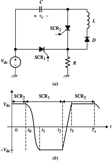
Fig. P3.34
-
3.35
Figure P3.35 shows a DIAC-TRIAC switching circuit used in a heater controller, motor speed variation and light dimmer applications. Design for R and RL so that the TRIAC triggers at 30° and 210° during the positive and negative cycles, respectively. Assume v s(t) = 110 sin 2 π60t and the DIAC breakover voltage is 24 V.
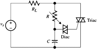
Fig. P3.35
-
3.36
Assume the switch is turned on at t = 0 and the capacitor was initially discharged in the circuit of Fig. P3.36. Derive the expression for v C(t) and sketch it for 0 < t < 40 ms, where v s(t) = 110 sin 2 π50t, R = 10 kΩ, and C = 1 μF.
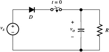
Fig. P3.36
-
3.37
Figure P3.37 shows a self-oscillating LC circuit that allows the SCR to turn off naturally without using an additional auxiliary SCR. This circuit is known as a series resonant turnoff circuit. (a) Derive the expression for v C(t) and i L(t). (b) Determine the power rating of the SCR. Assume the SCR is first triggered at t = 0 and repeatedly every T = 2 ms. Assume v C(0−) = 30 V and i L(0−) = 0.
Fig. P3.37
-
3.38
The circuit given in Fig. P3.38 represents one possible implementation of a family of dc-dc converters known as soft-switching converters.
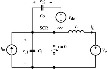
Fig. P3.38
-
(a)
If we assume the switch is turned ON at t = 0, show that the capacitor voltage for t > 0 is given by:
$$ {v}_{\mathrm{c}1}={V}_o+\left({V}_{dc}-{V}_o\right)\cos {\omega}_ot $$where \( {\omega}_o=\sqrt{C_{\mathrm{eq}}L} \) and C eq = C 1 + C 2.
-
(b)
In order to turn S back on while the capacitor voltage across C1 is zero, the voltage across it must be allowed to reach zero again during the off-time of the switch. Show that for zero-voltage switching to occur, the following condition must be met:
$$ {V}_{\mathrm{o}}<\frac{V_{dc}}{2} $$
-
(a)
-
3.39
Figure P3.39 shows output and input waveforms in a cycloconverter-type power electronic circuit, where the output frequency is one-half of the input voltage frequency. Find the Fourier series representation for such waveform.
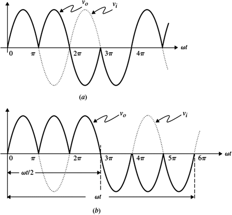
Fig. P3.39
-
3.40
Figure P3.40 shows a typical inductor current waveform in a switch-mode power supply when operating at the boundary of continuous and discontinuous mode operations. (a) Determine the Fourier components for i(t), (b) calculate its average and rms values, and (c) calculate the THDi.
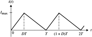
Fig. P3.40
-
3.41
Repeat Problem 3.40 for the inductor current shown in Fig. P3.41, which represents a discontinuous conduction mode of operation in a switch-mode power supply.
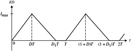
Fig. P3.41
-
3.42
Figure P3.42 shows a half-wave rectifier waveform with a sine-squared pulse represented mathematically for 0 < t < T/2 by the following equation:
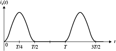
Fig. P3.42
$$ {i}_{\mathrm{s}}(t)={I}_{\mathrm{o}}{\sin}^2\omega t $$-
(a)
Determine the Fourier coefficients.
-
(b)
Calculate the rms and THD i values.
-
(a)
-
3.43
Consider a sinusoidal line current shown in Fig. P3.43 that can be represented mathematically for 0 < t < T by the following equation:
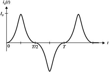
Fig. P3.43
$$ {i}_{\mathrm{s}}(t)={I}_{\mathrm{o}}{\sin}^n\omega t $$where n is an odd integer. By assuming that the line voltage is given by v s(t) = V s sin ωt V, derive the expression for the power factor the THDi.
-
3.44
The simplified equivalent circuit of a dc-dc converter known as a buck converter is shown in Fig. P3.44a. Assume the switch is turned on and off according to the waveform shown in Fig. P3.44b Sketch the steady-state waveforms for v sw, i sw, and i o and derive the expression for the average output power.
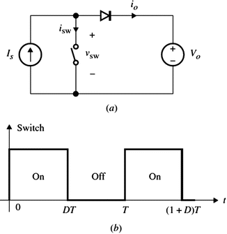
Fig. P3.44
-
3.45
Figure P3.45 shows eight different switch-mode topologies of which only one topology is valid. Identify such topology and state which circuit law (KVL or KCL) is being violated for each of the other topologies.
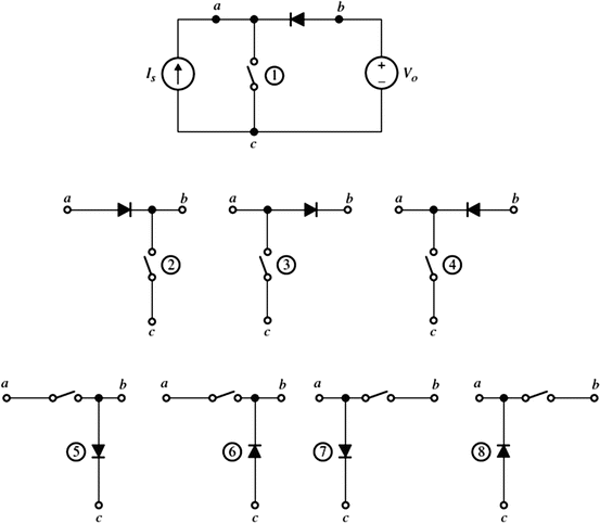
Fig. P3.45
-
3.46
Sketch the waveforms for i D1, i D2, v o and find the average output voltage for the circuit of Fig. P3.46a, where v s1(t) and v s2(t)are shown in Fig. P3.46b.
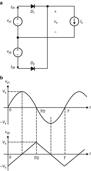
Fig. P3.46
-
3.47
Repeat Problem 3.46 by replacing D 1 and D 2 by two switches S 1 and S 2 as shown in Fig. P3.47. Assume that S 1 is conducting only when |v s1(t)| > V s/3 and S 2 is the complement of S 1.
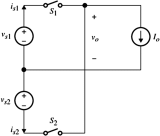
Fig. P3.47
-
3.48
Consider the full-bridge rectifier of Fig. P3.48 with a current source i s(t) = I s sin ωt and a constant output voltage, V o. Sketch v s and i o, and find the average output power.
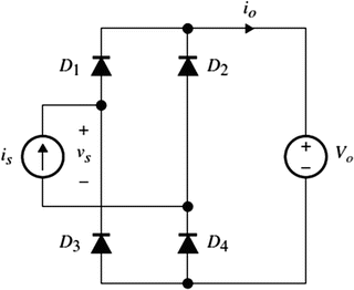
Fig. P3.48
-
3.49
Consider the full-bridge rectifier of Fig. P3.49 with a voltage source v s(t) = V s sin ωt and a constant output current, I o. Sketch i s and v o and find the average output power.
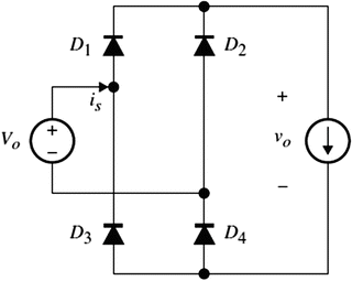
Fig. P3.49
-
3.50
Figure P3.50 shows four different switch-mode topologies of which only one topology is valid. Identify such topology and state the circuit law (KCL or KVL) that is being violated for each of the other topologies.
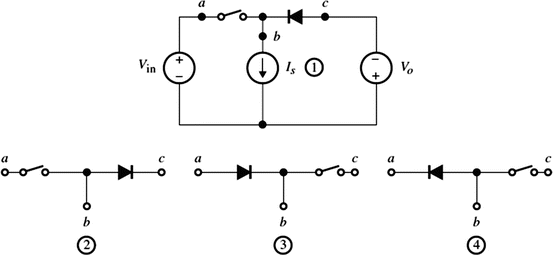
Fig. P3.50
-
3.51
Figure P3.51a shows an equivalent circuit for a switch-mode converter—Cuk (pronounced chook). Show that the ratio between the average output voltage, V o, and the average input voltage, V in, is given by the following relation:
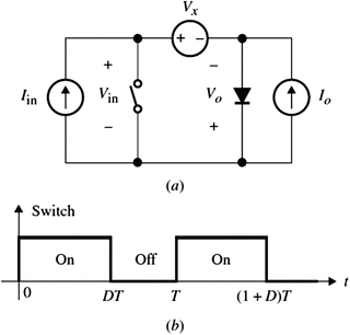
Fig. P3.51
$$ \frac{{\boldsymbol{V}}_0}{{\boldsymbol{V}}_{\mathbf{in}}}=\frac{\boldsymbol{D}}{1-\boldsymbol{D}} $$The switch waveform is shown in Fig. P3.51b.
Hint: Use the average voltage V x as given by V in − V o .
-
3.52
Figure P3.52a shows a switch-mode power electronic converter known as the buck-boost converter. This circuit is used to convert a DC input voltage to another dc level at the load. If we assume that the inductor, L, is large and the average output current is represented by a constant current source, then the equivalent circuit becomes as shown in Fig. P3.52b. Assume the switch is turned on and off as shown in Fig. P3.52c. Figure P3.52a show that the capacitor current is given in Fig. P3.52d, b sketch the steady-state average capacitor voltage.
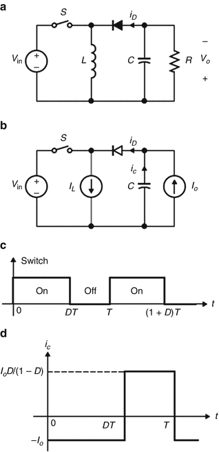
Fig. P3.52
-
3.53
Determine the power factor for the circuits given in Problems 3.48 and 3.49.
-
3.54
Consider a transformer with a turn ration N 1/N 2 = 200, and rated at 240 kVA (44 kV ⁄ 220 V) used to step down a 60 Hz voltage in a distributed system.
-
(a)
Determine the rated primary and secondary currents.
-
(b)
Determine the load impedance seen between the primary terminals when the load is fully loaded.
-
(a)
-
3.55
Consider the periodical current waveform shown in Fig. P3.55.
Determine its RMS expression. If you can only reduce one of the duty ratios D1, D2, and D3 by 10%, determine which one will give you the smallest reduction in RMS value.


Fig. P3.55
Rights and permissions
Copyright information
© 2018 Springer International Publishing AG
About this chapter

Cite this chapter
Batarseh, I., Harb, A. (2018). Switching Circuits, Power Computations, and Component Concepts. In: Power Electronics. Springer, Cham. https://doi.org/10.1007/978-3-319-68366-9_3
Download citation
DOI: https://doi.org/10.1007/978-3-319-68366-9_3
Published:
Publisher Name: Springer, Cham
Print ISBN: 978-3-319-68365-2
Online ISBN: 978-3-319-68366-9
eBook Packages: EngineeringEngineering (R0)