
Abstract
In the future, electronics will face many challenges beyond the prediction of Moore’s law. In this context, nanopackaging will play a crucial role for enabling future electronics to be consistent with future component, system, and circuit board (or global-level) requirements. Moreover, assembly approaches are moving toward heterogeneous three-dimensional integrated circuits (3D ICs) with silicon via wafer thinning, bonding technologies, and 3D system integration and miniaturization. Many of these packaging and assembly requirements are triggering an unprecedented pace of innovation in terms of new technologies, new system integration techniques, and new materials. Intensive research investigations are focused on carbon nanotubes (CNTs), graphene, 2D materials, nanowires, nanoparticles, and so on. In addition, many challenges remain to be faced with regard to the development of state-of-the-art interconnect interfaces, the development of predictive modeling tools based on multidisciplinary and advanced multiscales approaches, and the fabrication and tests of representative demonstrators with a significant impact.
The work described in this chapter is in this context. We propose innovative CNTs based on high-frequency interconnections as microbumps. A demonstration of a successfully CNT-based flip chip bonded structure is performed at high frequencies up to 40 GHz. Very encouraging measurements and the dedicated hybrid (EM/analytical) model are in good agreement. We propose that CNT-based microbumps should be a new alternative interconnect for future submillimeter electronics.
1 Introduction
Radio frequency (RF) packaging in electronics combines all assembly techniques in order to build with the best accuracy, repeatability, and stable RF systems. The combination of active and passive devices forms the RF system. Interconnections connect all blocks (subsystems, chips) together in order to mesh the entire system. Thus, interconnections play a major role in the functioning of the entire RF system. Interconnections need to bring the power and the signal with the lowest losses possible and the shortest delay reachable. With the increase of the frequency, the interconnections need to be more and more compact with a constant degree of performance.
Moore’s law predicts that transistor sizes will continue to linearly decrease in future electronics chips. Hence, smaller interconnections on the first and second level will be necessary (Fig. 8.1). Currently, metallic interconnections are used in conventional high-frequency electronics up to the microscale. However, bulk materials such as metals have serious limitations at both the nano and micron scales (such as electromigration and grain scattering issues). Indeed, with a low current density below 20 nm, metal behaviour is not suitable for using as interconnections in terms of performance and mechanical, thermal constraints. To overcome such limitations, CNTs could be a perfect candidate for interconnections because of their remarkable properties such as their long mean free path and their high current-carrying capability.

Level 1 and level 0 of interconnections. Level 1 connects the entire chip while the level0 interconnections are smaller and only bond unique components together such as transistors
Two main levels of interconnection exist in integrated circuits: the first and second (also called level 0) levels regard their size, length, and purpose (Fig. 8.1). The first level lists all “chip-to-chip packaging” interconnects such as wire bonding, the flip chip, or a via-hole. These are used to connect the chip to its package and are the principal interest of the work presented in this chapter. On the other hand, we have the back-end-of-line interconnection (BEOL), which lists all smaller interconnections other than the first level. These are usually located in the integrated circuits themselves.
1.1 Level 0 of Interconnection Using CNTs
Interconnections bring both the signal and the power to electronics components. Interconnections at level 0 are split into two categories because the interconnections to bring a signal do not have the same technical requirements (size, material, etc.) as the interconnections for power. Moreover, these interconnections are indexed into three categories according to their length: local interconnects for the smallest length, semiglobal interconnects and global interconnects for the bigger lengths. Most simulations have been performed on interconnects to verify if the use of CNTs in interconnections is able to outperform the performance of current metallic interconnections. Most work (e.g., modeling and fabrication) so far with CNTs has been focused on level 0 [1, 2].
1.1.1 Local Interconnections Using CNTs [3]
-
(a)
Local Interconnects: Properties and Issues
Because electronics are at the edge of the nanoscale, the size of the smallest interconnects in integrated circuits will necessarily shrink in the future. Indeed, they will be the most affected interconnections due to the size reduction of the electronic circuits themselves. This reduction in size will cause some problems, such as how to develop fabrication tools and equipment small enough to manipulate nanoscale components (e.g., nanoscale lithography, etc.) as well as electromigration issues (e.g., grain boundary scattering, surface scattering, and a high resistive diffusion barrier layer) that will occur with bulk materials at the nanoscale.
The length of the local interconnects is short (500–1500 nm). However, after they are aggregated, their length usually becomes larger. That is the reason why, today, 50 % of the interconnect power is dissipated at local interconnects. One of the main issues to solve with local interconnects is lateral capacitance. This high capacitance decreases the performance of interconnects by increasing the transmission signal delay. On the other hand, to carry the power to interconnects, the smallest resistance is necessary, which implies a thicker interconnect; this also avoids the electromigration effect. Thus, we will see how CNT bundles are able to solve these issues when approaching the nanoscale.
-
(b)
Local Interconnects: Performance of CNTs (SW vs. MW) [2, 4]
Simulations have shown that controlled-diameter single-wall CNTs (SWCNTs) are able to lower the lateral capacitance by a factor of four and the power dissipation by a factor of two compared to a metallic local interconnect. This improves the speed of the interconnect by 50 %. Indeed, by controlling the number of CNTs in a given area, we are able to decrease the total lateral capacitance by decreasing the number of CNTs in the bundle. The SWCNT diameter can be also decreased (lower CNT surface) in order to slow down the lateral capacitance. But to bring the power to local interconnects, because of an important quantum resistance that exists in an individual CNT, it is necessary to keep a minimum of parallel CNTs. This will have the effect of decreasing the total interconnect resistance. Thus, a trade-off between the capacitance and resistance needs to be investigated regarding the CNTs’ bundle density. Finally, because of the short lengths of the local interconnects (i.e., below the value of the CNT mean free path), CNT resistance remains high compared to a copper wire, for example, and may not be suitable for this level of interconnects.
1.1.2 Semi-Global Interconnections Using CNTs
The length of the semiglobal interconnects is logically located between the local and global interconnects, that is, between a few micro and hundreds of microns. These interconncts represent only a small proportion of interconnections length. Regarding the state of these interconnects, densely packed double-wall CNT (DWCNT) bundles are preferred. Indeed, because the product R × C (where R is the interconnect resistance and C is the interconnect capacitance) determines the delay, an important number of CNTs with the lowest capacitance are necessary, and thus DWCNTs are preferred over SWCNTs due to the higher proportions of metallic CNTs that we are able to achieve with current fabrication processes.
1.1.3 Global Interconnections Using CNTs
Global interconnects have a length higher than a few hundred microns. They are mostly made from aluminum or copper. Using these materials, the resistance becomes proportional to the square root of the materials. With CNT bundles and the correct density of CNTs, we are able to decrease the width of the interconnections made by metal. However, a relatively large density of CNTs is necessary in order to reach a total interconnection resistance lower than a metal wire. If we use the SWCNTs instead of multiwall CNTs (MWCNTs), a perfect control of the CNT chirality during the growth needs to be done in order to get only metallic ones. An expected control of the CNTs chirality during the growth has so far not been achieved.
At the global level, for the same reasons as the local interconnects level, capacitance in CNT bundles can be easily lower than the metal interconnections, especially because the interconnect width at this level is larger. Finally, the inductance in CNT interconnections includes both kinetic and magnetic inductance effects. The kinetic inductance effect will be very low and can be neglected because of the large number of CNTs in parallel in the bundle. The magnetic inductance remains the same as the metal interconnection. So, at the global level of interconnects, physical models have shown that a bundle of large diameter (50 nm) MWCNTs could be used for power distribution because of their lower resistance, whereas dense SWCNT bundles (with at least 40 % of metallic SWCNT) can outperform the signal interconnect made by metal. The percentage of metallic versus semiconducting CNT is the major issue for the use of SWCNT in interconnects. A CNT density as high as 9.1015/m2 has been obtained [5].
1.1.4 Conclusion
In conclusion, CNTs (both SW and MW) have pros and cons for use in these three levels of interconnection. According to the dimensions of the interconnections (length, diameter, etc.), CNT bundles with the correct density and type of CNTs may be able to outperform the performance of metal interconnections. Finally, CNTs would be an optimal material for a multilevel interconnect network by combining carbon-based structures. However, the state of the art shows us that the types of interconnections made by CNTs still need to be improved on the CNT growth control in order to integrate in future devices. So far, several CNTs bundles have been successfully fabricated for IC applications.
1.2 Level 1 of Interconnection Using CNTs [4, 6–8]
We now present the connections from the chip to it package. These interconncts play a major role in packaging because they need to deal with powering, cooling, and protecting electronic components in RF systems. Not surprisingly, the performance, size, cost, and reliability of the packaging—and more precisely the interconnections—will be strongly dependent on both the material used and the method employed (e.g., wire bonding, flip chip, via hole).
As with the local and global interconnections presented previously, because of the scaling down of transistor sizes in integrated circuits, further miniaturization will be necessary for interconnection. Three-dimensional packaging will increase the level of integration in electronics, and in this part of the discussion, we focus on using wire bonding, via hole and flip chip technologies. These three methods to interconnect a chip to an IC have a high degree of integration; however, their use involves a manufacturing process dealing with both thermal and reliability issues. Shrinking the interconnect size will even further complicate the fabrication process.
Thus, it becomes important to discover new materials with unique and excellent properties compatible with the nanoscale. CNTs may be a solution for off-chip interconnections used for signal and power transmission, in the same way as local and global interconnects. Moreover, because most of the time these interconnects “feed” an entire chip, they are more exposed to thermal and mechanical constraints. Again, the solution may come from CNTs and their unique mechanical, electrical, and thermal properties.
1.2.1 Wire Bonding
Wire bonding has been the most-used technology so far and the first way discovered to interconnect integrated circuits. The wire is usually made of gold (but can also be made of copper or aluminum) with a minimum diameter of 15 μm. We encounter two major problems with this type of interconnection. First, integration is not optimal because the wire has a length between 200 and 400 μm located around the chip. Secondly, the wire has a very low diameter (15 μm), which implies a high magnetic inductance. So, the use of wire bonding technology may be an issue above 50 GHz because of this high magnetic inductance.
1.2.2 Hot-Via [9–11]
This second interconnection configuration, called hot-via, is based on flip chip technology. Instead of flipping the chip in order to interconnect it from the topside, the backside is directly interconnected. Thus, a metallic bump links first the motherboard with the backside of the IC, and a via is then connected through the substrate to the IC. This technology maintains the advantages of allowing a glance on the IC as well as the possibility of realizing a transition between the coplanar accesses on the motherboard to a microstrip line on the chip. For the bumps, metals such as copper and gold are currently employed. Thus, size reduction of the chip will still affect them, and the use of CNTs as the via hole transition may be an answer of the downscaling issues.
1.2.3 Flip Chip
In recent years, much research has focused on compact designs, 3D integration, and high operation frequency in electronics. Flip chip is one of the technologies offering lower insertion loss [12], compact packages [13] and low-cost fabrication [14], but such requirements are limited at higher frequencies (i.e., higher than 100 GHz) because of the size limitation of the interconnection. As the name of the technology suggests, the flip chip consists of flipping the chip/IC and connecting the back face with the motherboard by metal bumps. In contrast with the hot-via presented previously, the back face of the chip, where the integrated circuit is, is connected. No vias through the substrate are necessary and only a planar technology is sufficient to make the flip chip compatible. This advantage of topology avoids the issues of via growth with CNTs and thus simplifies the steps of the fabrication process. IBM first introduced flip chip interconnections in 1970. At that time, flip chip technology was called C4 (controlled collapse chip connection).
Today, flip chip technology is widely used throughout the industry and is used daily in many electronics devices. To meet the demands of compact-size multifunctional designs at higher frequencies, metal bumps need to be downscaled. However, downscaling metal bumps in the microscale range is highly susceptible to electromigration issues, hence affecting adjacent devices or causes reliability issues [15] as already presented with local and global interconnections.
-
(a)
Flip Chip Using CNTs (State of the Art)
The use of vertical CNT bundles as flip chip bumps is an alternative approach for overcoming this problem and proposes interesting capabilities. Indeed, compared to gold, an ideal CNT is able to reach an electrical conductivity three times higher and a mean free path up to 25 orders of magnitude larger [4]. Its large kinetic inductance and a negligible magnetic inductance [4] also allow CNT to have a negligible skin depth effect. Another advantage of using CNTs for interconnection is their high current-carrying capacity (109 A/cm2) and their excellent thermal conductivity (3000 W m−1 K−1) [16], potentially giving a better thermal management and power dissipation to a flip chip structure.
According to the International Technology Roadmap for Semiconductors, the forecasted requirement for flip chip bump pitches will shrink below 20 μm. However, traditional solder bumps encounter difficulties downscaling below 30 μm pitch due to the high diffusive and softening nature of solder [17], electromigration, and grain scattering issues [15]. CNTs are a suitable choice for future flip chip interconnections [4]. These advantages have motivated researchers and our group to evaluate the performance of CNT bumps for interconnect usage in both DC and high-frequency applications [4, 18]. Thus, a combination of both flip chip and CNT has the potential to make devices workable beyond 100 GHz with high performance. Indeed, in the literature for flip chip technology, we cannot find interconnections with a diameter lower than 20–25 μm [19, 20] working at a higher frequency than 100 GHz.
Much work on CNT bumps has been performed in recent years, and Soga et~al. reported low DC resistance of 2.3 Ω for a 100-μm diameter bump [21]. But only a few works have presented a flip-chip-based technology. Flip chip using CNT bundles as bumps for a high-power amplifier was presented in [20] by Iway’s group (Fig. 8.2). They showed a high-density (1011 cm−2) CNT bundle as a bump for flip chip technology. Gold was plated on the surfaces of patterned metal and CNT bumps to allow thermal-assisted flip chip bonding bumps. A temperature of 345 °C was then necessary to fix the flip chip. The bundle diameter was 10 μm and the bundle resistance was found negligible because of the high number of CNTs.
Fig. 8.2 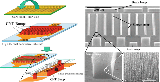
On left, concept of a flip chip using carbon nanotube interconnections for thermal management. On right, SEM images of the corresponding CNT bundles. A high CNT density is observed. Source: [20]
As we can see in this work, flip chip technology coupled with CNTs is able to exhibit a good heat-removal technology. Indeed, the thermal management in interconnects requires new material and new approaches at the nanoscale. CNT-based flip chip technology could be a very efficient method. A flip chip interconnect was also presented by Hermann et~al. using CNT pads on one side and metal contact pads on the other [18]. However, to realize a permanent mechanical contact, the bumps were filled with epoxy and heated to 200 °C to achieve 2.2 Ω bumps resistance. Hermann et~al. demonstrated a reliable electrical flip chip interconnect using CNT bumps working over 2000 temperature cycles [18]. In all the works above, the CNT bumps were grown using the chemical vapor deposition (CVD) approach. The mechanism for vertical alignment during the thermal CVD approach is achieved mainly by the electrostatic and van der Waals forces between CNTs, resulting in tubes that are not exactly “aligned” [22]. Poor “alignment” forms bends, reduces the mean free path, and increases the resistance of CNT [23]. Plasma-enhanced chemical vapor deposition (PECVD) is able to solve this issue by introducing an electric field to achieve alignment as well as lower the growth temperature [16].
To summarize, a high aspect ratio (with CNT bundle diameter below 20 μm) is necessary to get good performance with the increase of frequency. High aspect ratio CNT bumps are reachable for better high-frequency performance. Lower process temperatures need to be reached, and beyond proof of the flip chip concept by 3D interconnected CNTs, future devices with a better control of density and a higher density will be suitable to increase the number of CNT contacts. Finally, another problem encountered in nanopackaging concerns the solder. Indeed, mechanical and thermal constraints become too high at a very low scale to support such a process. Thus, the idea of using a contact between CNTs and the electrostatic and van der Waals forces as the mechanical solder will be presented later.

2 CNT-Based Microbumps
In the flip chip scenario, the grown CNT bumps are usually pressed onto prepatterned conductive adhesive [21] or solder materials [24] to form the connections we saw in the previous part. This approach requires heating up the structure to a minimum of 200 °C in order to reflow the materials to obtain good contacts. Yung et~al. [25] demonstrated a large-scale assembly process using vertically aligned CNT interconnection bundles showing that CNTs adhere well to each other by van der Waals forces and electrostatic interactions. However, no work using CNT interconnection bumps was reported for a CNT bump pitch below 150 μm, which is a requirement for future flip chip technology.
In the present work, we demonstrate the CNT interconnection bump-joining methodology for a pitch smaller than 150 μm. The fabrication methodology is divided into three parts:
-
1.
Fabrication of the structure dedicated to RF application;
-
2.
Growth of CNT bumps on both sides of the substrate using the PECVD approach;
-
3.
Alignment and “insertion of the CNT bumps into each other using a flip chip bonder machine.
The first flip chip device working up to 40 GHz is fabricated and is characterized to set up and optimize the process and finally to demonstrate proof of the proposed innovative approach to interconnect CNTs. Moreover, we discuss the technological aspects of developing the test structure, and will present the DC and RF behaviour of small-scale CNT interconnection bumps. Finally, modelling using electromagnetic (EM) and hybrid EM/analytic approaches will be conducted in order to extract CNT parameters and understand the electrical behaviour of the test device. Then we will present a theoretical approach to flip chip working up to 110 GHz.
2.1 CNT Growth on Gold Metallization
As will be explained later, in order to fabricate CNT-based flip chip bonding, we need to develop CNTs directly on Au metallization. Consequently, one of the issues encountered during the process is the controllability of CNT growth density on Au as well as the understanding of interaction between different barrier layers and Au underlayers. Gold inhibits CNT growth, and thus a study for suitable barrier layers is required between the catalyst and Au metallization [26]. CNT growth has been reported to be influenced by different types of barrier layers: Titanium (Ti), titanium nitride (TiN), and chromium (Cr) were reported to support CNT growth, while aluminum (Al), Ni–Cr alloy, Cu, and Au inhibit growth [26–28]. The reason for using different barrier layers depends on the needs of applications; TiN is claimed to be the best barrier layer on Cu, whereas Ti and Cr are common barrier layers used to improve the adhesion of Au on Si and in the under-bump metallization for bumps [28, 29].
2.1.1 Test Structure
The test structure consists of 50-Ω coplanar waveguide (CPW) with a length of 0.7 mm for the signal (center) and 1.2 mm for the ground (Fig. 8.3). The line and bump patterns are obtained using photolithography techniques, as we will detail in the next part. First, 700 nm of thermal oxide is grown at 1200 °C on high-resistivity Si wafers (>10 kΩ cm). The high-resistivity wafer is necessary for the microwave applications. Next, 10 nm Ti is used as an adhesion promoter followed by depositing 1-μm thick Au metallization lines. These two layers are deposited using an e-beam process. Using the lift-off approach, 50-μm diameter bumps are formed followed by 50-nm barrier layer and 20-nm nickel (Ni) catalyst deposition.

Schematic of coplanar waveguides (CPW) test structure used (not drawn to scale). Left shows the top view of the CPW with a length of 0.7 mm for signal and 1.2 mm for ground. The dark circles indicate the locations of the CNT interconnects. Right shows the cross-section view indicating different layers of the test structure. Note that the 50 nm barrier layer is not shown in this figure
All metal depositions are carried out using the e-beam evaporation technique at room temperature, and TiN is sputter-deposited at 75 °C. The final CNT growth process is performed at 8 mbar inside a PECVD chamber. The growth process includes pretreatment of the Ni catalyst in NH3 environment for 2 min at 800 °C. The growth is carried out for a duration of 15 min using C2H2 as the carbon feedstock gas at a 4:1 ratio. The cathode voltage is biased at −707 V providing a DC plasma power of 100 W. Ex situ characterizations are carried out using the LEO 1550 Gemini scanning electron microscope (SEM) for a CNT structure at different stages, and 532 Renishaw Visible Raman for Raman analysis. The RF measurements are done using a probe station connected to an Agilent HP 8510C network analyzer. The test environment is calibrated using short-open-load-thru scheme in order to remove the losses from the setup (cables, connectors, vector network analyzer (VNA), etc.) and S-parameters are extracted for the range of 1–20 GHz with a step of 0.1 GHz.
2.1.2 Results and Discussion
The influence of CNT growth parameters on Au metallization lines is observed at various stages of the growth process as shown in Fig. 8.4. Figure 8.4a shows the morphology of the deposited Au metallization, which is smooth with no cracks under the observation of SEM. As a reminder, the Au is deposited with e-beam equipment with a process temperature always below 70 °C. Figure 8.4b shows the morphology of Au metallization after being subjected to high-temperature processing at 800 °C in ambient NH3, resulting in the formation of crack lines. Finally, Fig. 8.4c shows the surface roughening of the Au metallization after exposure to C2H2 feedstock gas and plasma treatment. The Au has agglomerated and formed a hill-like structure. De Los Santos et~al. [30] suggested that the top layer of the Au melted, and that Au atoms diffused and nucleated at new sites. The addition of plasma at 800 °C raised the surface energy and likely induced the melting of the top layers of Au.

SEM micrographs of the Au metallization at different stages of CNT growth. (a) Au-deposited film is smooth with no crack-lines. The circular islands are formed during the deposition of Au metallization by e-beam evaporation process. (b) After annealing for 2 min at 800 °C in ambient NH3 and crack-lines are observed. (c) After subjecting to C2H2 and plasma treatment for 15 min in a PECVD chamber, the Au film formed a hill-like morphology
Using a two-point probe technique, the resistance of the Au coplanar strips lines registered an initial resistance of 2.03 and 7.73 Ω after the PECVD process. The increase in resistance is likely the result of film cracking and the formation of eutectic composition at the Au interface during annealing at 800 °C [31]. Thus, from the SEM micrographs and two-point probe testing, it is shown that the Au lines have degraded and suffered as a result of the CNT growth process.
Despite the structural degradation of the Au coplanar lines, experimental S-parameter properties shown in Fig. 8.5 are acceptable. To eliminate errors due to physical differences between test structures during the fabrication processes, the same coplanar structures (A and B) are used at every stage of measurements. Figure 8.5a, c show the return loss parameter (S11) and insertion loss parameter (S21) of test structure A, respectively, whereas Fig. 8.5b, d refer to measurements from test structure B. Each individual graph includes measurements at three different stages, namely, (1) the As-deposited film, (2) after 2 min annealing in ambient NH3, and (3) after 15 min of CNT growth.

S-parameters of the two test structures A and B: (a) return loss of structure A; (b) return loss of structure B; (c) insertion loss of structure A; and (d) insertion loss of structure B. Note that the peaks at 1 GHz in each S-parameter results above are due to the calibration process for the probe station. The calibration shows no successful results at this frequency
The results show that the cracks formed on the Au metallization after annealing caused the S-parameters measurements to worsen as compared to the As-deposited coplanar lines in Fig. 8.5. Insertion losses (S21) decrease by 1.5–2 dB and a degradation equal to 5 dB is visible on the S11 reflection parameter. However, the line performances were still correct between 1 and 20 GHz. Interestingly, the same test structures show improvement as compared to the annealed case after being subjected to the plasma effect. After plasma treatment, the S11 reflection parameter had improved and behaved like the Au-deposited lines (highest peak at −17 dB for structure A and −19 dB for structure B).
Moreover, the S21 transmission parameter of the coplanar line was also improved by an average of 1.87 dB for structure A and 1.32 dB for structure B as compared to the annealed lines. The observed results have two possible explanations: plasma could improve the quality of the line by cleaning off native oxide or amorphous carbon and/or plasma increases the surface energy of the Au lines leading to surface change at the Au metallization and forms new agglomerated structure, which presents new channels to carry the signal [32, 33].
2.2 RF Flip Chip Test Structure Based on CNT Bumps
2.2.1 Design and Fabrication
-
(a)
Description of the Test Structure
In order to demonstrate proof of high-frequency CNT-based flip chip bonding, we designed a simple test structure composed of a 50-Ω CPW flip chip bonded on a substrate carrier. The topology of the signal line on the substrate carrier is optimized to compensate for the parasitic capacitance that occurs between the two substrates. All the dimensions are given in Fig. 8.6. An entire modelling (EM and hybrid EM/analytical) of the device was done including CNT interconnections in order to extract some CNT properties such as the contact resistance between CNTs. To demonstrate the feasibility of using the PECVD approach for achieving fine-pitch CNT bumps, three different sets of test structures comprised of (Structure 1) 170 μm by 150 μm, (Structure 2) 120 μm by 100 μm, and (Structure 3) 70 μm by 50 μm CNT bumps size are designed (Fig. 8.6)
Fig. 8.6 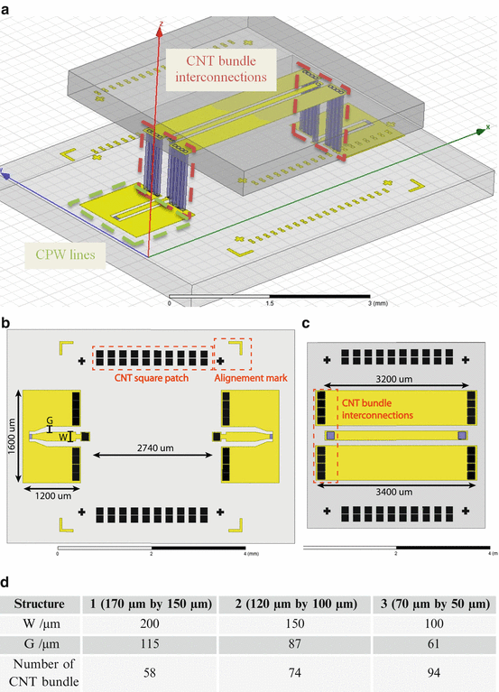
Schematic of the flip chip structure fabricated to test for both DC and RF functionality. (a) The final flip chip after the chip is flipped and combined with the carrier; (b) carrier design that comprises an “open” coplanar line structure; (c) chip design that comprises of coplanar line; (d)shows the variation of the size of three flip chip test structure
In order to improve the mechanical support of the test structure, we introduced rows of dummy CNT bumps positioned at the sides of the chip and die to increase the densities of the CNT bumps. The dummy bumps provided additional mechanical support to hold the weight and levelled the attached die.
-
(b)
Design: Hybrid (EM/Circuit) Modelling
The flip chip test structure is studied applying a hybrid approach based on 3D EM/circuit modelling between 1 and 40 GHz. This modelling combines full EM simulation and an analytical model of the CNT bundles. The analytical model depends on several parameters such as CNT diameter, CNT length, bundle CNT density and CNT components that will be described later. An optimization of the flip chip performance becomes possible as well. All the structures, except the CNT bumps, are considered by 3D EM simulations in order to define a generalized matrix [SG]. [SG] is defined between input/output ports (port 1 and port 2) and internal lumped accesses (3–6) for connecting circuit models of CNT bumps (Figs. 8.7 and 8.8).
Fig. 8.7 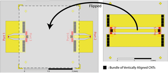
Top view of the schematic of the flip chip structure
Fig. 8.8 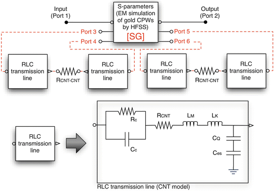
Diagram of the hybrid flip chip structure model
Electromagnetic simulations are performed with the software Ansoft HFSS. In Fig. 8.8, [SG] represents the matrix extracted from EM simulation of the flip chip structure. The “RLC transmission line” box corresponds to the CNT bundle model that will be presented in the following discussion. RCNT−CNT is the contact resistance between interconnected CNTs.
The circuit model based on an RLC transmission line describing the electrical behaviour of the CNT structure is presented in Fig. 8.8. The CNT circuit models are inserted between the lumped accesses (ports 3–4 and ports 5–6) of the flip chip matrix [SG]. The RLC transmission line is composed of lumped and distributed components as described in [34]. Briefly, the contact capacitance CC and the contact resistance RC model the contact between the CNTs. The metal and values are found according to this other work [35]. The quantum resistance of RCNT is considered equal to 20 kΩ/μm in comparison with previous experimental work [36]. The two other distributed components for nanowire effects are a kinetic inductance \( {L}_k={L}_{k- bundle} = \frac{h}{2{v}_F}\times l\times \frac{1}{N_{i- channel}\times {N}_{CNT}} \) and a quantum capacitance \( {C}_Q={C}_{Q- bundle} = \frac{2{e}^2}{h{v}_F}\times l\times {N}_{i- channel}\times {N}_C \) where (vF = 9.7 × 10⁵ m/s: Fermi’s velocity). According to the physical properties of the CNTs we consider in our test structure, there are Ni-channel = 374 in our model. The magnetic inductance LM is considered negligible compared to the very high kinetic inductance Lk in nanowires [34]. Electrostatic capacitance CES represents the coupling effect between the ground plane and the CNT. According to the experimental CNT we consider, CES and CQ can be neglected. At last, in order to model a bundle of CNTs, we also consider the coupling between weak CNTs because of the large distance between them (about 200–500 nm). Then, the RLC CNT models are placed in parallel according to the estimated number of CNTs in the bundle, NMWCNT = 1.35 × 10⁵. All components values are visible in Table 8.1
Table 8.1 CNT bundle components values As explained, all the lumped elements are defined according to the ideal technological properties of the CNT bundles, and will be used to design the whole test structure that will be fabricated. At this stage of modelling, the contact resistance between two CNTs, RCNT–CNT, is considered equal to zero. It will be extracted after the flip chip process and will allow us to define an accurate hybrid (EM/analytical) model of the test structure. We will present later how the value of RCNT–CNT is extracted. Such a model will be used to understand and optimize the behaviour of the test structure.
-
(c)
Fabrication Process of the Test Structure
The fabrication is carried out using standard lithography and a metal deposition system. A schematic of the process is presented in Fig. 8.9.
Fig. 8.9 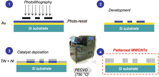
Photolithography, e-beam, and PECVD steps to deposit pattern a catalyst material before CNT growth by PECVD. (1) Shows the UV illumination of the photo resist using a shadow mask. (2) Shows the development of the photo resist in order to remove nonwanted patterns. (3) Is the deposition of the barrier layer and catalyst on the all sample by e-beam. Finally, in (4) the CNTs are grown by PECVD and the entire photo resist is removed in order to keep only the remaining bundle of CNTs
The substrate is a 4-in.-high resistivity (HR) <100> wafer with resistivity >10 kΩ. The use of an HR wafer is necessary in RF application to minimize attenuation losses. Next, the wafers are cleaned and placed into the tube furnace to perform wet oxidation of 600 nm of SiO2. The use of the SiO2 layer is not necessary for RF application, but from a DC point of view, it is necessary to reduce the leakage current. Next, lithography patterning is performed to create the opening for the depositing of Au or Cu metallization by e-beam evaporation. After the first metallization is completed, a second lithography step is performed for the catalyst (used for CNT growth) and its barrier layer is required for CNT growth [37–39]. The final 4-in. wafer is then cut up using a dicing machine and is ready for the growth of CNT. The CNT growths are then carried out in the Aixtron Black Magic PECVD deposition system at 650 °C with a plasma power of 85 W for 30 min. The growth pressure is at 6 mbars with a gas ratio of gas of 1:5 (C2H2:NH3).
From the literature point of view, there have been reports that using NH3 during growth results in N-doped CNT. The NH3 function is necessary to act as an etchant source and possibly as N-dopants according to various group [40, 41]. CNT bumps height of ~20 μm is obtained as shown in Fig. 8.10. Each of these CNT bumps comprises of MWCNT with an average diameter about100 nm.
Fig. 8.10 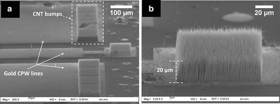
(a) Low-magnification view of CNT bumps formed on the Au metal lines. (b) SEM image of a CNT bump grown using the PECVD approach. The grown CNTs were vertically aligned and their length was approximately 20 μm
Subsequently, a Panasonic flip chip bonder machine is used to perform the die alignment and attachment. The top part of the flip chip is flipped at 180° above the bottom part and a downward force is applied (Fig. 8.11). A load setting from 0.5 to 3 kg with a bonding time of 30 s is used as the bonding parameter.
Fig. 8.11 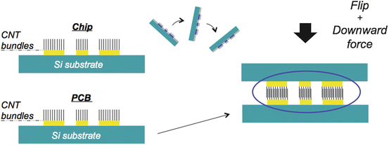
Principle of the flip chip using interconnected bundle of carbon nanotubes. Top part (chip or die) is rotated at 180° above the bottom part (PCB or carrier) and a downward force is applied on it. CNTs will stick together by the electrostatic and van der Waals forces
The bonding load of 0.5 kg is sufficient to cause the CNT from the bottom carrier to “insert” and touch the top die. The load of 0.5 kg, which is equivalent to 4.5 N or 3.125 kg/cm2, is much lower than that applied in previous reported flip chip experiments [18, 20, 21]. However, the load of 1.5 kg is found to provide the optimum electrical properties. Indeed, a higher electrical resistance is obtained when a low load (0.5 kg) is applied on it [39]. We believe that the CNTs start to be compressed when a larger load is used (greater than 1.5 kg), just as in the work of [21].
Indeed, with a load of 3 kg, we obtained the higher rate of successful devices, but the achieved resistances were all higher than the one measured with an applied load of 1.5 kg. We believe the compression increased the depth of penetration and the chances of CNTs contacting with one another (Fig. 8.12). After the bonding process is completed and the load is removed, CNTs return to their original vertical configuration. No bonding temperature is used in our experiment. Finally, we notice that the mechanical adhesion between the two parts is good enough to carry and measure our structures in DC/RF, but too weak to perform a stress test of the device. Thus, an improvement of the mechanical adhesion between the two flip chip parts needs to be investigated.
Fig. 8.12 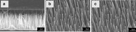
Interconnection length regarding the force applied: (a) no load, (b) 0.03 g, and (c) 3 kg. At 3 kg, the interconnection length is maximal


2.2.2 Fabrication Results
To demonstrate the feasibility of using PECVD approaches to achieve fine-pitch CNT bumps, three different sets of test structures (Fig. 8.13) are fabricated. The SEM images in Fig. 8.13 show the CNT bumps grown using the PECVD approach allows pitch sizes down to 80 μm (70 μm bump size + 10 μm distance between two bumps) in our experiment. Homogenous CNT bump heights can also be observed throughout the carrier and die (dummy and CNT bumps on electrodes). Larger catalyst pattern geometry would result in longer CNT length due to the differences in partial pressure of carbon feedstock gas. However, the effect of catalyst pattern geometry is not significant in this experiment, and the height of all CNT bumps is assumed to be 20 μm regardless of the bumps dimensions.

The CNT bumps on an Au electrode with three different pitches. The smallest pitch designed is 80 μm. The dimension of each CNT bump in (a) structure 1 is 170 μm × 150 μm, (b) structure 2 is 120 μm × 100 μm, and (c) structure 3 is 70 μm × 50 μm. The scale bar at the bottom right of each image represents 100 μm
Thus, for the first time, CNT interconnection bump joining methodology for fine-pitch bumps is achieved, as shown on Fig. 8.14. In Fig. 8.14a, the flip chip test structure is observed at an angle of 75° under the SEM. The assembled final structure, as shown in Fig. 8.14b–d, is separated by an average distance of 20–25 μm as observed in the SEM micrograph. It is also observed that some CNTs are able to reach the opposite part and be in contact with it, creating alternative paths to the CNT–CNT interconnections. A combination of both contacts could improve the device performance. Due to the equipment limitations, microphotographs of the CNT bumps during the bonding and release process could not be performed to demonstrate the mechanical flexibility of CNT bump as observed by [21]. However, based on the SEM images in Fig. 8.14c–f, the vertical alignment of CNT bump can still be observed, which is likely due to the mechanical flexibility of CNT bumps. In this experiment, structures 1 (170 × 150 μm bump size) and 2 (120 × 100 μm bump size) are tilted to 75° in the SEM to observe the gap between test structures. This is remarkable because no bonding temperature or adhesive is used during the bonding process to mechanically bond the die to the carrier.

SEM images of the CNT interconnection bumps demonstrated using a flip chip concept (a–f). The dimensions of CNT bumps were 100 μm × 100 μm for all images. (a) Die attached to a carrier at a tilted angle of 75°; (b) magnified view of two CNT interconnection bumps; (c–d) show the distance separating the two parts of the flip chip; (e) CNTs from bottom carrier are observed to be touching the die substrate indicative of the connections made; and (f) shows the CNTs touching each other
The attached die is subsequently removed from the carrier using a tweezers to observe the effect of the CNT bumps after bonding. The carrier and die are then loaded into the SEM chamber with the same orientation to observe the condition of the CNT bumps that are in contact with one another, as shown in Fig. 8.15. Aportion of the CNT bump appeared to be smeared as seen from Fig. 8.15a, but a high percentage of CNT bump retained their original structure. This is similar to [25] observations for a large-scale CNT-to-CNT interconnection structure, which demonstrates that the bonding process is reworkable.

SEM images of the CNT bumps morphology after removal of the top die. (a) CNT bumps on the carrier; (b) CNT bumps on the chip joined to the carrier bump in (a, c) with a magnified view of the bump. The remaining vertical alignments of the CNTs show the mechanical flexibility of CNTs
2.2.3 DC Measurements: CNT Bump Resistance and Reworkability
In order to extract the resistance of a single CNT bump resistance, a four-point DC technique is used. The main advantage of using the four-point probe design is to eliminate the contact resistance of the probe pins and metal lines, thus removing unwanted resistance from the measurements. The resistance of the metallization is found to be in the same order as the CNT bumps resistance in our experiments. We have to consider it during the extraction of the CNT bump resistance. For improving the electrical performance of the CNT interconnections bumps on metal, the choice of barrier layer is crucial. Using Ti and TiN as the barrier layer in our study, Ti/TiN is found to be a better choice as compared to using TiN barrier layer. This is due to better conductivity of Ti and Ti is a preferred choice of adhesive layer for various metals in the industries.
In Fig. 8.16, it is also observed that the resistance decreases when the barrier layer thickness decreases. It further shows that electrons tunnel through the barrier layer and affect CNT conductivity. By comparing the resistivity values, the resistivity extracted are 0.164 Ω cm for the 30 s Ti/30 s TiN, 5.175 Ω cm for the 3 min Ti/60 s TiN and 0.695 Ω cm for 5 min TiN barrier layer. This clearly shows that thinner barrier layers help to improve the CNT conductivity. Due to the measurement technique, Fig. 8.16 shows the total resistance between the input and output accesses. Consequently, the two resistances of both input and output signal bumps are considered and are supposed to be the same. Later in this work, we will consider the case that gives the lowest bump resistance equal to 6.25 Ω.

I-V measurements—resistance of CNT bumps on three different barrier layers. The results on 30 s Ti_30 s TiN gives the lowest bump resistance equal to 6.25 Ω
In addition, we studied the effect of the bonding load. The relationship between the bonding load and resistance are plotted and shown in Fig. 8.17. The solid square and dots symbols represent the average resistance of one CNT interconnection and the standard errors are plotted as the error bars. Two observations can be made from the experiment. First, when the bonding load increases, the depth of penetration increases and the gap between the top chip and carrier decreases as shown in the inset. SEM image shown that the distances between the chip and carrier reduce from 35 μm (at 1 kg) to 30 μm (at 2 kg) to 28 μm (at 3 kg).

Relationship between the measured resistances and bonding load. The SEM images as shown in the inset show the decreasing gap (distance) between the top chip and substrate with increasing bonding load
Second, an increase in the loading weight leads to a decrease of the resistance in an exponential manner. The variation of resistance also fluctuates less above 2 kg as indicated by the error bars. The decrease in measured resistance is mainly due to the increase in the number of parallel paths for electron transfer from one CNT to another. As CNT have large elastic modulus, a minimum load will be require to deform the CNT and to increase the number of conducting paths [42]. Below the optimum loading weight, CNT demonstrate resilient and flexibility which can return to its original position after bending [21]. The measured resistance is thus highly dependent on the probability to form conducting paths that result in the large error bar. Above the minimum load, the vertically aligned CNT starts to bend and form contacts between its neighboring CNT of the top chip, which creates more parallel paths for electrons transfer, thus reducing the measure resistance. When the CNT to CNT interspacing distances is decreased, the resistance also decreased [43]. The adhesion between CNT to CNT are solely by van der Waals forces interactions[25].
It is very important for the CNT interconnection bump to be reworkable in order to save cost. To verify our measurement repeatability, the top chip is removed and bonded again to the same carrier. The measurements are compared and shown in Fig. 8.18. The slight deviation of the second attempt could be caused by the differences in chip placement due to the limited alignment accuracy of the bonding machine. Figure 8.18b–d shows the SEM images of the CNT bumps after repeated bonding which are still intact.

(a) I-V characteristics after repeated bonding; (b) SEM image of the carrier after repeated bonding; (c) SEM image of the chip after repeated bonding; (d) the vertical alignment within the CNT bumps can still be observed in both structures
2.2.4 RF Measurements: Discussion
High-frequency measurements from 1 to 40 GHz are also performed on the flip chip structures. Measurements are run with a VNA Agilent HP8510C and 150-μm pitch Cascade Microtech Infinity probes. A thru-reflect-line (TRL) calibration process is done before each measurement with a maximum error bar equal to 0.1 dB. TRL is a calibration process done before a high-frequency measurement by a VNA. This calibration process consists of replacing the device under test by a thru line, a short circuit, and finally a load circuit at 50 Ω.
As shown in Fig. 8.19 two identical test structures (device a and b) with a 170 × 150 μm bump size exhibit a S21 parameters of −1.21 and −3.69 dB from 1 to 40 GHz. The return loss (S11) stayed below −13 dB. The small variations above 30 GHz are due to the calibration process, which returns a measurement error between 0.1 and 0.2 dB on some frequency points.

S-parameters measurements of the flip chip device a (solid lines) and device b (dash lines) between carrier input and output
At this experimental stage, proof of high-frequency CNT-based flip chips is demonstrated. The experimental results are encouraging.
In addition, to complete the experimental analysis on RF behaviour, we proceed to the estimation of the CNTs bump insertion losses. Thus, before we realize the flip chip process, we measure up to 40 GHz the S-parameters of the bonded CPW after the PECVD process. The length of the CPW top line is 3.2 mm. Insertion losses remain near −1 dB while the return losses remain below −20 dB. For instance, at 20 GHz, the top line insertion losses were −1.6 dB. Considering that the total length between the input and output accesses of the flip chip test structure is equal to 5 mm, we can estimate that the insertion losses due to the CPW line only are equal to −2.5 dB (−1.6 dB for a length of 3.2 mm). As shown in Fig. 8.19, the insertion losses of the test structure are near −2.5 dB. We can also deduce that the insertion losses due to CNT bumps only are negligible at higher frequencies. The same comparison can be made on all the measurement frequency bands.
Even if experimental results are encouraging, they present low performance compared to the classical approach with classical metal bumps. In the future, we need to fully understand and optimize not only their high-frequency behaviour, but also their mechanical properties.
To summarize, we have demonstrated the first measurement of a flip chip technology based on an interconnected bundle of CNTs from DC to 40 GHz. An innovative way to interconnect CNTs similar to the Velcro principle is used with successfully mechanical and electrical adhesions. No underfill or heat is necessary to interconnect the CNT bundles, which decreases the number of process steps and the cost of the device. The bumps size is 170 × 150 μm and only composed by 100-nm-diameter MWCNTs. This first measurement gives encouraging performance for using CNTs to replace metal bumps in flip chip technology. Moreover, a bonding repeatability is observed in DC, which opens the door to a new type of device: CNT interconnected bumps can be flipped several times and it becomes possible to replace a defective component or to verify components in a complex environment. However, the performances are still lower than metal bumps at this frequency range.
Future devices with a better control of density and a higher density will be suitable to increase the number of CNT–CNT contacts. A densification of the CNT bundle after bonding can also be a solution to increase the CNT density and so decrease the distance between CNTs. We can imagine changing the CNT bundle geometry in order to increase the surface in contact between the two flip chip parts. A better optimization of the access lines would also increase the performance of the device. The CNT growth temperature also needs to be reduced in the future. Atemperature lower than 350 °C will be reached soon and will allow us to create a fully CMOS-compatible flip chip device based on CNT interconnections. Finally, we need to carry on mechanical and temperature stress tests in order to verify the resistance of our device in an aggressive environment.
2.2.5 Hybrid (EM/Analytical) Modelling
In order to understand the physical phenomena involved in the flip chip interconnect. and also to extract an accurate hybrid model, high-frequency simulations are done. We will first extract from measurements and theoretical definition all the parameters of the CNT bump equivalent model. This model is described in Fig. 8.20 which shows the model of the CNT bumps we measured in DC whevn considering the flip chip test structure (see Sect. 8.2.2.3). This model will permit us to extract the unknown contact resistance RCNT–CNT between two CNTs.

(a) Side view of the flip chip structure and the corresponding equivalent electrical circuit with a breakdown of the bump resistances; (b) details on Rbump corresponding to the bump resistance for two interconnected MWCNTs according to the (a) schematic
Rbump is the DC resistance of the bump. From measurements in Sect. 8.2.2.3 we found Rbump equal to 6.25 Ω. R′ resistance represents the linked CNT parts, whereas R″ resistance represents the nonlinked part. Finally, RCNT−CNT is the contact resistance between two MWCNTs. The contact resistance RC is found according to the work of [35]. The resistances R″ and R′ can be estimated from previous works done under similar conditions [36]. Consequently, knowing approximately the number of CNTs in a bundle (1.35 × 10⁵), RCNT–CNT can be extracted. This contact resistance between two MWCNTs RCNT−CNT is equal to 324 kΩ. This value is similar to the one found in the work of other group [44].
This resistance will then be added to the analytical CNT model we presented previously in Sect. 8.2.2.1.b, in order to model the entire flip chip structure using the hybrid EM/analytical approach. All component values can be found in the Table 8.1. As shown in Fig. 8.21, good agreement is found between hybrid modeling and measurements. Consequently, the model is validated.

S-parameters of the flip chip structure measured between port 1 and port 2. Solid lines correspond to the measurements while dashed lines show the hybrid EM/circuit simulation results
The hybrid model is used to perform parametric studies of the test structure by modifying the number of CNTs, their composition, their resistance, and other CNT parameters. Several tests are done to determine the effects of the bump resistance RCNT and of the contact resistance RCNT–CNT. By improving the CNT fabrication process, RCNT will decrease and the performances will be slightly improved. For instance, considering RCNT equal to 10 kΩ/μm (instead of 20 kΩ/μm in Table 8.1) the transmission level is only improved of 0.5 dB. We modify also RCNT–CNT. Again, we observe very few effects on the behaviour of the test structure. For instance, by dividing by three RCNT–CNT, we only improved the transmission level by 0.5 dB at low frequency (1 GHz) and by 0.25 dB at a higher frequency (40 GHz). With RCNT–CNT = 10 kΩ, we improve S21 by 0.75 dB on all the bandwidth. Thus, we observed that decreasing the contact resistance between CNTs alone is not sufficient for improving more than 0.5 dB the S21 parameter.
In conclusion, even if an important work needs to be done on the CNT qualities by improving the fabrication process, it won’t be sufficient to get a significant improvement of the electrical behaviour. So finally, we modify the number of CNTs in the bundle from 0.13 × 10⁶ CNTs to 1.106 CNTs. In this case, the transmission level increases significantly of about 1.5 dB at low frequency (1 GHz) to 1 dB at higher frequency (40 GHz). Indeed, by increasing the number of CNTs in parallel, two resistances decrease at the same time: the contact resistance RCNT–CNT (more contacts in parallel) and the equivalent resistance due to the CNTs in parallel. The behaviour is very close to the optimum case we can expect for an ideal bump. In conclusion, focusing on the CNT density (or number of CNTs in a bundle) might be the best choice to improve the RF performances of the bump interconnect.
3 Conclusion and Future Work
The feasibility of using the PECVD approach to achieve CNT bumps pitch smaller than 150 μm was studied. The introduction of TiN barrier layer between Ni catalyst and Au metallization allows an efficient growth of CNT bumps directly on Au while maintaining good electrical connections between CNT and Au electrodes. The successful growth of CNT on Au metallization opens up opportunities to evaluate the performance of vertically aligned CNT bundles in very high frequency domain. The proof of concept of innovative RF CNTs bump flip chip is demonstrated. A test structure is built and tested. For the first time, very encouraging CNT-based flip chip measurements are obtained from DC up 40 GHz. In addition to the experimental work, a theoretical study based on 3D EM simulation and the hybrid EM/analytical approach was done. Electrical parameters of the CNT bumps were extracted for better understanding.
We conclude that even if the process and the current electrical performances need to be improved, many advantages exist such as the high aspect ratio, the possibility to flip several times, the lack of underfill, and so on. Suggestions to improve the process and electrical performances have been proposed.
In addition, we aim to extend this proof in the submillimeter wave domain. Indeed, at high frequencies, to realize small size bumps with metal (smaller than 20 μm in diameter) is challenging because of electro-migration effects and low current density capabilities [45]. Thus, we expect that above 100 GHz, CNT bumps should outperform metal bumps due to their excellent electrical conductivity for becoming an alternative technology compared to a current one. From the previous study, we consider a new test structure operating around 100 GHz. The new structure is identical to the one described in Fig. 8.6, with new dimensions suitable for submillimeter wave applications. The size of the bump is 20 × 20 × 20 μm. As shown on Fig. 8.22, we apply parametric studies based on the hybrid EM/circuit model described previously.

Simulated S21-parameters from 80 to 120 GHz with several numbers of MWCNTs in a 20 × 20 μm bump (from 2400 to 500,000 MWCNTs)
From this parametric study, we observe that 2400 MWCNTs is not enough to have acceptable submillimeter performances (red dash curve). By increasing the number of CNTs in the bundles, we observe that with NMWCNT = 1.105 and 2.105 (blue and black dashes), we have already enough CNTs to achieve insertion loss better than −4 dB and return loss below −10 dB. By increasing the number of CNTs to NMWCNT = 5.105 (purple dash curve) we can even reach the same performance we obtained with ideal bumps (perfect metal). This represents a CNT density of 1.25 × 10¹⁵ CNT m−2, which is a realistic density. In conclusion, an increase of the CNT density is essential in order to achieve a correct level of performance for submillimeter application. Thus, CNTs become credible candidates to outperform metal interconnections for flip chip technology. A fabrication of the test structure is currently under progress.
References
Naeemi A, Meindl JD (2008) Performance modeling for single- and multiwall carbon nanotubes as signal and power interconnects in gigascale systems. IEEE Trans Electron Devices 55:2574–2582
Banerjee K, Hong L, Srivastava N (2008) Current status and future perspectives of carbon nanotube interconnects. In: Proceedings of the 8th international conference on nanotechnology, NANO ‘08, IEEE, Arlington, TX, 18–21 August 2008, pp 432–436
Saraswat P (2002) http://www.stanford.edu/class/ee311/NOTES/Interconnect Scaling.pdf
Hong L, Chuan X, Srivastava N, Banerjee K (2009) Carbon nanomaterials for next-generation interconnects and passives: physics, status, and prospects. IEEE Trans Electron Devices 56:1799–1821
Awano Y, Sato S, Nihei M, Sakai T, Ohno Y, Mizutani T (2010) Carbon nanotubes for VLSI: interconnect and transistor applications. Proc IEEE 98:2015–2031
Zhengchun L, Lijie C, Kar S, Ajayan PM, Jian-Qiang L (2009) Fabrication and electrical characterization of densified carbon nanotube micropillars for IC interconnection. IEEE Trans Nanotechnol 8:196–203
Nihei M, Kawabata A, Sato M, Nozue T, Hyakushima T, Kondo D, Ohfuti M, Sato S, Yuji A (2010) Carbon nanotube interconnect technologies for future LSIs. In: Swart JW (ed) Solid state circuits technologies. InTech, Rijeka
Jiang D, Wang T, Chen S, Ye L, Liu J (2013) Paper-mediated controlled densification and low temperature transfer of carbon nanotube forests for electronic interconnect application. Microelectron Eng 103:177–180
Ting J-H, Chiu C-C, Huang F-Y (2009) Carbon nanotube array vias for interconnect applications. J Vac Sci Technol B Microelectron Nanometer Struct 27:1086–1092
Wen W, Krishnan S, Ke L, Xuhui S, Wu R, Yamada T et al (2009) Extracting resistances of carbon nanostructures in vias. In: IEEE international conference on microelectronic test structures, ICMTS 2009, IEEE, Oxnard, CA, 30 March 2009–2 April 2009, pp 27–30
Xuhui S, Ke L, Wu R, Wilhite P, Yang CY (2010) Contact resistances of carbon nanotubes grown under various conditions. In: Proceedings of the 2010 IEEE nanotechnology materials and devices conference, IEEE, Monterey, CA, 12–15 October 2010, pp 332–333
Sangsub S, Youngmin K, Jimin M, Heeseok L, Youngwoo K, Kwang-Seok S (2009) Amillimeter-wave system-on-package technology using a thin-film substrate with a flip-chip interconnection. IEEE Trans Adv Packag 32:101–108
Hsu LH, Oh CW, Wu WC, Chang EY, Zirath H, Wang CT et al (2012) Design, fabrication, and reliability of low-cost flip-chip-on-board package for commercial applications up to 50 GHz. IEEE Trans Compon Packag Manuf Technol 2:402–409
Heinrich W (2005) The flip-chip approach for millimeter wave packaging. IEEE Microw Mag 6:36–45
Jae-Woong N, Kai C, Suh JO, Tu KN (2007) Electromigration study in flip chip solder joints. In: Proceedings of the 57th electronic components and technology conference, ECTC ‘07, IEEE, Reno, NV, 29 May 2007–1 June 2007, pp 1450–1455
Chhowalla M, Teo KBK, Ducati C, Rupesinghe NL, Amaratunga GAJ, Ferrari AC et al (2001) Growth process conditions of vertically aligned carbon nanotubes using plasma enhanced chemical vapor deposition. J Appl Phys 90:5308–5317
Tummala R, Wong CP, Markondeya Raj P (2009) Nanopackaging research at Georgia Tech. IEEE Nanotechnol Mag 3:20–25
Hermann S, Pahl B, Ecke R, Schulz SE, Gessner T (2010) Carbon nanotubes for nanoscale low temperature flip chip connections. Microelectron Eng 87:438–442
Jentzsch A, Heinrich W (2001) Theory and measurements of flip-chip interconnects for frequencies up to 100 GHz. IEEE Trans Microw Theory Tech 49:871–878
Iwai T, Shioya H, Kondo D, Hirose S, Kawabata A, Sato S et al (2005) Thermal and source bumps utilizing carbon nanotubes for flip-chip high power amplifiers. In: IEEE international electron devices meeting, 2005 IEDM technical digest, IEEE, Washington, DC, 5–5 December 2005, pp 257–260
Soga I, Kondo D, Yamaguchi Y, Iwai T, Mizukoshi M, Awano Y et al (2008) Carbon nanotube bumps for LSI interconnect. In: Proceedings of the 58th electronic components and technology conference, ECTC 2008, IEEE, Lake Buena Vista, FL, 27–30 May 2008, pp 1390–1394
Fan S, Chapline MG, Franklin NR, Tombler TW, Cassell AM, Dai H (1999) Self-oriented regular arrays of carbon nanotubes and their field emission properties. Science 283:512–514
Jun H, WonBong C (2008) Controlled growth and electrical characterization of bent single-walled carbon nanotubes. Nanotechnology 19:505601
Kumar A, Pushparaj VL, Kar S, Nalamasu O, Ajayan PM, Baskaran R (2006) Contact transfer of aligned carbon nanotube arrays onto conducting substrates. Appl Phys Lett 89: 163120–163123
Yung KP, Wei J, Tay BK (2009) Formation and assembly of carbon nanotube bumps for interconnection applications. Diam Relat Mater 18:1109–1113
Wang B, Liu X, Liu H, Wu D, Wang H, Jiang J et al (2003) Controllable preparation of patterns of aligned carbon nanotubes on metals and metal-coated silicon substrates. J Mater Chem 13:1124–1126
Tay BK, Wang ZF, Yung KP, Wei J (2008) Effects of under CNT metallization layers on carbon nanotubes growth. Mod Phys Lett 22:1827–1836
García-Céspedes J, Thomasson S, Teo KBK, Kinloch IA, Milne WI, Pascual E et al (2009) Efficient diffusion barrier layers for the catalytic growth of carbon nanotubes on copper substrates. Carbon 47:613–621
Bertrand N, Drevillon B, Gheorghiu A, Senemaud C, Martinu L, Klemberg-Sapieha JE (1998) Adhesion improvement of plasma-deposited silica thin films on stainless steel substrate studied by X-ray photoemission spectroscopy and in situ infrared ellipsometry. J Vac Sci Technol A 16:6–12
De Los Santos VL, Lee D, Seo J, Leon FL, Bustamante DA, Suzuki S et al (2009) Crystallization and surface morphology of Au/SiO2 thin films following furnace and flame annealing. Surf Sci 603:2978–2985
Wißmann P, Finzel H-U (2007) The effect of annealing on the electrical resistivity of thin gold films. In: Electrical resistivity of thin metal films, vol 223. Springer, Heidelberg, pp 35–52
Basa D (2010) Plasma treatment studies of MIS devices. Cent Eur J Phys 8:400–407
von Arnim VL, Fessmann J, Psotta L (1999) Plasma treatment of thin gold surfaces for wire bond applications. Surf Coat Technol 116–119:517–523
Burke PJ (2002) Luttinger liquid theory as a model of the gigahertz electrical properties of carbon nanotubes. IEEE Trans Nanotechnol 1:129–144
Minghui S, Zhiyong X, Yang C, Yuan L, Chan PCH (2011) Inductance properties of in situ-grown horizontally aligned carbon nanotubes. IEEE Trans Electron Devices 58:229–235
Yang C, Zhiyong X, Philip CHC (2010) Horizontally aligned carbon nanotube bundles for interconnect application: diameter-dependent contact resistance and mean free path. Nanotechnology 21:235705
Kociak M, Suenaga K et al (2002) Linking chiral indices and transport properties of double-walled carbon nanotubes, vol 89. American Physical Society, Ridge, NY
White CT, Mintmire JW (2004) Fundamental properties of single-wall carbon nanotubes. JPhys Chem B 109:52–65
Yap CC, Tan D, Brun C, Teo EHT, Wei J, Baillargeat D et al (2011) Characterization of novel CNT to CNT joining interconnections implemented for 1st level flip chip packaging. Presented at the electronics packaging technology conference, Singapore
Susi T, Kaskela A, Zhu Z, Ayala P, Arenal R, Tian Y et al (2011) Nitrogen-doped single-walled carbon nanotube thin films exhibiting anomalous sheet resistances. Chem Mater 23:2201–2208
Kim J-B, Kong S-J, Lee S-Y, Kim J-H, Lee H-R, Kim C-D et al (2012) Characteristics of nitrogen-doped carbon nanotubes synthesized by using PECVD and thermal CVD. J Korean Phys Soc 60:1124–1128
Yaglioglu O, Hart AJ, Martens R, Slocum AH (2006) Method of characterizing electrical contact properties of carbon nanotube coated surfaces. Rev Sci Instrum 77:095105–095103
Yoon Y-G, Mazzoni MSC, Choi HJ, Ihm J, Louie SG (2001) Structural deformation and intertube conductance of crossed carbon nanotube junctions. Phys Rev Lett 86:688–691
Fuhrer MS, Nygård J, Shih L, Forero M, Yoon Y-G, Mazzoni MSC et al (2000) Crossed nanotube junctions. Science 288:494–497
Nah J-W, Chen K (2007) Electromigration study in flip chip solder joints, Conference: Electronic Components and Technology Conference, 2007. ECTC '07. 1450–1455
Acknowledgements
The authors want to acknowledge all the contributors to this work and in particular Dr. Christophe Brun and Dr. Yap Chin Chong as main contributors during their Ph.D. thesis, Dr. Tan Chong Wei, Dr. Lu Congxiang, Dr. Chow Wai Leong, and Dunlin Tan for their help and valuable advice.
Author information
Authors and Affiliations
Corresponding author
Editor information
Editors and Affiliations
Rights and permissions
Copyright information
© 2017 Springer International Publishing Switzerland
About this chapter
Cite this chapter
Baillargeat, D., Tay, E.B.K. (2017). Carbon Nanotubes as Microbumps for 3D Integration. In: Todri-Sanial, A., Dijon, J., Maffucci, A. (eds) Carbon Nanotubes for Interconnects. Springer, Cham. https://doi.org/10.1007/978-3-319-29746-0_8
Download citation
DOI: https://doi.org/10.1007/978-3-319-29746-0_8
Published:
Publisher Name: Springer, Cham
Print ISBN: 978-3-319-29744-6
Online ISBN: 978-3-319-29746-0
eBook Packages: EngineeringEngineering (R0)