
Abstract
This section introduces some of the most common radio-frequency (RF) parameters used in the field of EMC and high-frequency circuit design and measurement. A particular emphasis lays on the term impedance matching and distinguishing between good and poor impedance matching.
The term impedance matching can be a very useful metaphor for connoting important aspects of social interactions. For example, the smooth and efficient functioning of social networks, whether in a society, a company, a group activity, and especially in relationships such as marriages and friendships, requires good communication in which information is faithfully transmitted between groups and individuals. When information is dissipated or “reflected,” such as when one side is not listening, it cannot be faithfully or efficiently processed, inevitably leading to misinterpretation, a process analogous.
—Geoffrey West
You have full access to this open access chapter, Download chapter PDF
Keywords
- RF parameters
- High-frequency parameters
- Reflection coefficient
- Voltage standing wave ratio (VSWR)
- Return loss
- Insertion loss
- Scattering parameters
- S-parameters
- Vector network analyzer
- Signal-to-noise ratio (SNR)
- Noise factor
- Noise figure
- 1 dB compression point (P1dB)
- Spectrum analyzer
- Superheterodyne analyzer
- Swept-tuned analyzer
- FFT analyzer
- Hybrid superheterodyne-FFT analyzer
- Resolution bandwidth
- Video bandwidth
- Quasi-peak detector
- Average detector
- Peak detector
- RMS detector
6.1 Reflection Coefficient \( \underline {\varGamma }\)
We speak of matched impedances in case the load impedance \( \underline {Z}_{load}\) is the complex conjugate of the source impedance \( \underline {Z}_{source} = \underline {Z}_{load}^{*}\) (Fig. 6.1). In radiated emission and immunity EMC testing, it is important to understand the term matching and how to quantify it. All EMC RF measurement test setup receiver and transmitter antennas must be matched to their receiver and transmitter equipment impedance (typically Z 0 = 50 Ω).

A one-port circuit and its reflection coefficient \( \underline {\varGamma }\). For a one-port \( \underline {\varGamma }\) is equal to the scattering parameter \( \underline {s}_{11}\)
The reflection coefficient \( \underline {\varGamma }\) is defined as [6]:
where:
-
\( \underline {V}_{forward} =\) complex forward voltage wave to the load in [V]
-
\( \underline {V}_{reflected} =\) complex reflected voltage wave by the load in [V]
-
\( \underline {Z}_{source} =\) complex source impedance in [Ω]
-
\( \underline {Z}_{load} =\) complex load impedance in [Ω]
The reflection coefficient Γ is often given in [dB]:
where:
-
P reflection = reflected power by the load in [W]
-
P forward = power sent to the load (at the load terminals) in [W]
6.2 Voltage Standing Wave Ratio (VSWR)
VSWR is dimensionless and means voltage standing wave ratio. The VSWR expresses the ratio of maximum and minimum voltage of a standing wave pattern along a transmission line. It is also a parameter for measuring the degree of impedance matching. Standing waves occur in case of impedance mismatch. A VSWR value of 1 means perfectly matched. A VSWR value of ∞ means complete mismatch (100% of the forward wave is reflected). Figure 6.2 shows an example of a standing wave pattern.

Example of a standing wave pattern along a transmission line (envelope curve of the sinusoidal forward wave \( \underline {V}_{forward}\) and its reflected wave \( \underline {V}_{reflected}\) of the same frequency)
The VSWR can be calculated by using the reflection coefficient from above [6]:
where:
-
|V |max = is the maximum value of the standing wave pattern in [V]
-
|V |min = is the minimum value of the standing wave pattern in [V]
-
\(| \underline {\varGamma }| =\) is the magnitude of the reflection coefficient
6.3 Return Loss (RL)
The return loss RL [dB] is a measure for the transferred power to a load by a source (Fig. 6.3). A low RL value indicates that not much power is transferred to the load and is reflected instead. Return loss [dB] is always a positive value and it is equal the reflection coefficient Γ [dB] multiplied by − 1 [5, 9].

Source with forward power P forward and the reflected power P reflected from a one-port circuit
where:
-
P forward = power sent to the load (at the load terminals) in [W]
-
P reflection = reflected power by the load in [W]
-
\(| \underline {\varGamma }| =\) is the magnitude of the reflection coefficient
6.4 Insertion Loss (IL)
The term insertion loss IL [dB] is generally used for describing the amount of power loss due to the insertion of one or several of the following components (passive two-port networks):
-
Transmission line (cable, PCB trace)
-
Connector
-
Passive filter
The insertion loss is the ratio in [dB] of the power P 1 and P 2 in Fig. 6.4. P 1 represents the power, which would be transferred to the load in case the source is directly connected to the load. The power P 2 represents the power, which is transferred to the load in case the passive two-port network is inserted between the source and the load [2, 6].
where:
-
P 1 = power, which would be transferred to the load in case the source is directly connected to the load (without passive two-port network) in [W]
Fig. 6.4 
Insertion loss
-
P 2 = power, which is transferred to the load in case the passive two-port network is inserted between the source and the load in [W]

6.5 Scattering Parameters
Scattering parameters —also called S-parameters—are commonly used in high-frequency or microwave engineering to characterize a two-port circuit (see Figs. 6.5 and 6.6). The scattering parameters describe the relation of the power wave parts \( \underline {a}_1\), \( \underline {b}_1\), \( \underline {a}_2\), \( \underline {b}_2\) that are transferred and reflected from a two-port input and output. The physical dimension for the incident \( \underline {a}\) and reflected \( \underline {b}\) power waves is not Watt, but it is \(\sqrt {\text{Watt}}\). The generic definitions for the forward power wave \( \underline {a}_i\) and the reflected power wave \( \underline {b}_i\) of an arbitrary port i are given as [1]:
where:
-
\( \underline {V}_i =\) complex voltage at the input of the ith port of a junction in [V]
Fig. 6.5 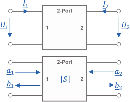
Scattering parameters of a two-port network
Fig. 6.6 
S-parameters are measured with vector network analyzers . The picture shows the R&S®ZNL6 by Rohde & Schwarz
-
\( \underline {I}_i =\) current flowing into the ith port of a junction in [A]
-
\( \underline {Z}_i =\) complex impedance of the ith port in [Ω]
-
\( \underline {Z}_i^* =\) complex conjugate of \( \underline {Z}_i\)
-
The positive real value is chosen for the square root in the denominators


The forward traveling power toward port 1 P 1fwd and the reflected power of port 1 P 1ref can be written as:
where:
-
\(\hat {V}_{1fwd} =\) peak value of the forward voltage to port 1 in [V]
-
\(\hat {V}_{1ref} = \) peak value of the reflected voltage from port 1 in [V]
-
\(\operatorname {Re}( \underline {Z}_1) =\) real part of the complex impedance \( \underline {Z}_1\) of port 1 in [Ω]
Generally speaking, the S-parameter \( \underline {s}_{ij}\) is determined by driving port j with an incident wave of voltage \(V_j^+\) and measuring the outgoing voltage wave \(V_i^-\) at port i. Considering Fig. 6.5, the four scattering parameters can be computed as follows:
where:
-
\( \underline {a}_1 =\) incoming power wave at the input port of a two-port in [\(\sqrt {W}\)]
-
\( \underline {b}_1 =\) outgoing power wave at the input port of a two-port in [\(\sqrt {W}\)]
-
\( \underline {a}_2 =\) incoming power wave at the output port of a two-port in [\(\sqrt {W}\)]
-
\( \underline {b}_2 =\) outgoing power wave at the output port of a two-port in [\(\sqrt {W}\)]
The formulas 6.12, 6.14, 6.13, 6.15 showed that the S-parameters can be determined by loading the ports with a reference impedance, e.g., Z 0 = 50 Ω. This means that \( \underline {s}_{11} = \underline {\varGamma }\) when the output port 2 is matched with its load. For a one-port \( \underline {s}_{11}\) is always equal the reflection coefficient \( \underline {\varGamma }\). The input reflection coefficient \( \underline {\varGamma }_{1}\) of a two-port with a certain load (given by the reflection factor \( \underline {\varGamma }_{L}\)) is given by:
6.6 Signal-to-Noise Ratio
The signal-to-noise-ratio SNR [dB] is a key figure in analog or digital signal processing applications. The bigger the SNR value, the better. The SNR is defined as the ratio of the desired signal power to the power of the undesired signal (noise, interference) [3]:
where:
-
P signal = power of the desired signal in [W]
-
P noise = power of the undesired signal (noise, interference) in [W]
6.7 Noise Factor and Noise Figure
Noise factor F and noise figure NF [dB] are measures of degradation of the signal-to-noise ratio (SNR), caused by components in a signal chain. The noise factor of a device (e.g., amplifier) is defined as the ratio of the SNR at the input of the device to the SNR at the output of the device [3]:
where:
-
SNRi = SNR of the signal at the input of the device (linear, not in [dB])
-
SNRo = SNR of the signal at the output of the device (linear, not in [dB])
The noise figure NF [dB] is defined as the noise factor F in [dB]:
where:
-
F = noise factor of the device (linear, not in [dB])
-
SNRi = SNR of the signal at the input of the device (linear, not in [dB])
-
SNRo = SNR of the signal at the output of the device (linear, not in [dB])
If several devices are cascaded (see Fig. 6.7), the total noise factor F can be calculated with Friis formula [3]:
where:
-
F n = noise figure of the n-th device (linear, not in [dB])
Fig. 6.7 
Cascade of devices with gain G n and noise factor F n
-
G n = gain of the n-th device (linear, not in [dB])

The first amplifier in a chain usually has the most significant effect on the total noise figure NF. Equation 6.21 shows that the first device should have the lowest noise factor F 1 and a high gain G 1, since the noise figure of any subsequent stage will be divided by the gains of the preceding stages. As a consequence, the noise figure requirements of subsequent stages are more relaxed.
The noise figure NF [dB] of a passive component (cable, attenuator, filter) is always its loss L, and one can set F = L and G = 1∕L (linear, not in [dB]) for a passive component [3], where G is the gain.
6.8 1 dB Compression Point
The 1 dB compression point P1dB [dB] is a key specification for amplifiers. Besides many factors, the gain G [dB] of an amplifier is a function of the amplifier’s input power P in [dBm]. P1dB is defined as the output power P out [dBm] (or sometimes as the input power P in) of an amplifier at which the output is 1 dB lower than it is supposed to be, if it were ideal. In other words, P1dB is the output power P out [dBm] when the amplifier is at the 1 dB compression point (Fig. 6.8).

1 dB compression point (P1dB) of an amplifier
Once an amplifier reaches its P1dB, it goes into compression and becomes a nonlinear device, producing distortion, harmonics, and intermodulation products. Therefore, amplifiers should always be operated below the P1dB.
6.9 Spectrum Analyzer Terms
Spectrum analyzers measure the power of a signal’s frequency components. Today, spectrum analyzers apply these measurement principles:
-
Superheterodyne. The analog measurement signal is mixed with a sweep generator frequency signal to the intermediate frequency IF, then band-pass filtered with the resolution bandwidth RBW (IF filter) and finally measured (envelop detector), low-pass filtered (VBW filter), and displayed (see Fig. 6.9a).
Fig. 6.9 
Block diagram of spectrum analyzer principles . (a) Superheterodyne principle. (b) FFT principle
-
FFT. The analog measurement signal is sampled and converted to a digital signal, where the FFT algorithm is used to calculate the frequency spectrum of that measurement signal (see Fig. 6.9a).

Basically, there are three types of spectrum analyzers:
-
Swept-tuned analyzers apply the principle of superheterodyne receivers. They have long scan times and a wide frequency range.
-
FFT analyzers apply the principle of the FFT. They have a limited frequency range and short scan times.
-
Hybrid superheterodyne-FFT analyzers combine the principle of superheterodyne measurement and FFT calculation. They have shorter scan times than purely swept-tuned analyzers and a wider bandwidth then FFT analyzers.
Sections 6.9.1–6.9.5 explain the basic terms of spectrum analyzers. Note: EMI receivers are spectrum analyzers that fulfill the requirements according to CISPR 16-1-1 [8] (dynamic range, peak-detection, etc.).
6.9.1 Frequency Range
A spectrum analyzer measures the input signal from the start frequency to the stop frequency . The frequency between the start and the stop frequency is called center frequency , and the difference is the frequency span .
6.9.2 Resolution Bandwidth
For spectrum analyzers that employ the superheterodyne principle, the resolution bandwidth (RBW) is the bandwidth of the band-pass IF filter in Fig. 6.9a. The RBW determines how close two signals can be resolved into two separate peaks. The smaller the RBW, the better the resolution in the frequency range and the lower the noise floor (see Fig. 6.10).

Measurement of the same signal with different resolution bandwidths (RBWs). Measurements performed with R&S®FSV3013 by Rohde & Schwarz. (a) RBW = 120 kHz. (b) RBW = 9 kHz
6.9.3 Video Bandwidth
For spectrum analyzers that employ the superheterodyne principle, the video bandwidth (VBW) is the bandwidth of the low-pass filter after the envelope detector in Fig. 6.9a. The VBW is used to discriminate between a low-power harmonic signal and the noise floor. The smaller the VBW, the smoother the envelope signal and the lower the noise floor (see Fig. 6.11).

Measurement of the same signal with different video bandwidths (VBWs). Measurements performed with R&S®FSV3013 by Rohde & Schwarz. (a) VBW = 200 kHz. (b) VBW = 1 Hz
6.9.4 Sweep Time
For spectrum analyzers that employ the superheterodyne principle, the sweep time t sweep [sec] is the time required to record the entire frequency range (span) [4]:
where:
-
k = Factor, depending on the type of filter and on the required level of accuracy
-
span = frequency range to be displayed in [Hz]
-
RBW = resolution bandwidth in [Hz]
-
VBW = video bandwidth in [Hz]
6.9.5 Detectors
Different detector types are used in spectrum analyzers (Fig. 6.12):
-
Quasi-peak detector. The quasi-peak detector determines the peaks of the measurement signal with a defined charge and discharge time [4]. Quasi-peak-detection mode is used for many RF emission measurements.
Fig. 6.12 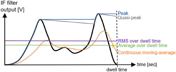
Spectrum analyzer detector types compared (symbolic picture)
-
Average detector. The average detector determines the linear average of the signal at the output of the IF envelope detector [7]. Many EMC RF emission measurements use average detectors.
-
Peak detector. The peak detector follows the signal at the output of the IF envelope detector and holds the maximum value during the measurement time (also called dwell time) until its discharge is forced [7].
-
RMS detector. The RMS detector determines the RMS value of the signal at the output of the IF envelope detector [7].

6.10 Summary
Table 6.1 summarize the impedance matching parameters and Table 6.2 compares the impedance matching parameters for matched vs. unmatched.
References
Kaneyuka Kurokawa. “Power Waves and the Scattering Matrix”. In: IEEE Transactions on Microwave Theory and Techniques Vol. 13.No. 2 (1965), pp. 194–202.
Mathieu Melenhorst Mark van Helvoort. EMC for Installers - Electromagnetic Compatibility of Systems and Installations. CRC Press, 2019.
Dr. Heinz Mathis. “Mobile Communications”. In: Fachhochschule OST (2003).
Measuring with Modern Spectrum Analyzers - Educational Note. Rohde & Schwarz GmbH & Co. KG. Feb. 2013.
Wendy M. Middleton. Reference Data For Engineers: Radio, Electronics, Computer and Communications. 9th edition. John Wiley & Sons, Inc., 2001.
Clayton R. Paul. Introduction to electromagnetic compatibility. 2nd edition. John Wiley & Sons Inc., 2008.
Specification for radio disturbance and immunity measuring apparatus and methods - Part 3: CISPR technical reports. International Electrotechnical Commission (IEC). 2010.
Specification for radio disturbance and immunity measuring apparatus and methods – Part 1-1: Radio disturbance and immunity measuring apparatus – Measuring apparatus. International Electrotechnical Commission (IEC). 2009.
Brian C. Wadell. Transmission line design handbook. Artech House Inc., 1991.
Author information
Authors and Affiliations
Rights and permissions
Open Access This chapter is licensed under the terms of the Creative Commons Attribution 4.0 International License (http://creativecommons.org/licenses/by/4.0/), which permits use, sharing, adaptation, distribution and reproduction in any medium or format, as long as you give appropriate credit to the original author(s) and the source, provide a link to the Creative Commons license and indicate if changes were made.
The images or other third party material in this chapter are included in the chapter's Creative Commons license, unless indicated otherwise in a credit line to the material. If material is not included in the chapter's Creative Commons license and your intended use is not permitted by statutory regulation or exceeds the permitted use, you will need to obtain permission directly from the copyright holder.
Copyright information
© 2023 The Author(s)
About this chapter

Cite this chapter
Keller, R.B. (2023). RF Parameters. In: Design for Electromagnetic Compatibility--In a Nutshell. Springer, Cham. https://doi.org/10.1007/978-3-031-14186-7_6
Download citation
DOI: https://doi.org/10.1007/978-3-031-14186-7_6
Published:
Publisher Name: Springer, Cham
Print ISBN: 978-3-031-14185-0
Online ISBN: 978-3-031-14186-7
eBook Packages: EngineeringEngineering (R0)