
Abstract
In order to choose the right components for EMI filters, it is essential to understand the properties and nonideal behavior of passive filter components. Therefore, in this chapter, the high-frequency behavior and other undesirable effects of conductors (wires, cables, PCB traces), resistors, capacitors, inductors, ferrite beads, common-mode chokes, baluns, varistors, and TVS diodes are presented.
We will make electricity so cheap that only the rich will burn candles.
—Thomas A. Edison
You have full access to this open access chapter, Download chapter PDF
Keywords
- Conductor
- Resistor
- Capacitor
- Inductor
- Ferrite bead
- Common-mode choke
- Balun
- Varistor
- TVS diode
- Gas discharge tube
- TVS thyristor
- Clamping device
- Crowbar device
- Internal inductance
- Internal impedance
- External inductance
- Total inductance
- High-frequency equivalent circuit
- Conductor equivalent circuit
- Capacitor temperature derating
- Capacitor voltage derating
- Capacitor aging
- Inductor saturation
- Inductor frequency response
- Cable mount ferrite bead
- Chip ferrite bead
11.1 Conductors
11.1.1 Definition of a Conductor
First, let us give a criterion for an electrical conductor and an insulator (dielectric material) [16]:
-
Conductor. \(\left (\sigma / \left (\omega \epsilon ' \right )\right )^2 \gg 1.0\)
-
Dielectric. \(\left (\sigma / \left (\omega \epsilon ' \right )\right )^2 \ll 1.0\)
where:
-
σ = specific conductance of the material in [S/m]
-
ω = 2πf = angular frequency of the sinusoidal signal in [rad/sec]
-
\(\epsilon ' = \epsilon _r^{\prime } \epsilon _0 =\) permittivity of the material in [F/m]
11.1.2 Conductor Equivalent Circuits
Figure 11.1 shows that the equivalent circuit of a single conductor is a simple RL-circuit, where the self-inductance L [H] is split into an internal and an external self-inductance:

Equivalent lumped-element circuit of a single conductor (no capacitance, because return current path and other parallel conductors are not considered)
where:
-
L = total partial inductance of a single conductor in [H]
-
L int = internal inductance of a single conductor in [H]
-
L ext = external inductance of a single conductor in [H]
-
Φ int(t) = internal magnetic flux of conductor caused by the current I in [Wb]
-
Φ ext(t) = external magnetic flux of conductor caused by the current I in [Wb]
-
i(t) = current through the conductor in [A]
Figure 11.2 shows that a single conductor has an internal H-field [A/m], but the internal E-field [V/m] is zero (nonexistent). Thus, a single conductor has an internal inductance L int [H] (linked to the internal H-field) but no internal capacitance (because of the missing E-field). In general, the internal inductance L int [H] is much smaller than the external inductance L ext [H]. This is especially valid for high frequencies (more details in Sect. 11.1.4).

Internal and external E- and H-field of a single round conductor with uniform current distribution (DC) in a homogeneous environment
At increasing signal frequency f [Hz], a conductor changes its impedance \( \underline {Z}(f)\) [Ω]. Sections 11.1.3–11.1.7 present the calculations of the high-frequency equivalent circuit parameters of the models shown in Fig. 11.1 (single conductor) and Fig. 11.3 (conductor and its return current path). Here is an explanation of the equivalent lumped-element circuit models:
-
Resistance. R′ [Ω/m] is the per-unit-length resistance and R = R′⋅ l [Ω] the resistance of a conductor with a certain length l [m].
Fig. 11.3 
Equivalent lumped-element circuit of a closed current loop (e.g., parallel conductors or PCB traces with forward and backward path). (a) Lumped-element π-model. (b) Lumped-element T-model
-
Internal self-inductance. \(L_{int}^{\prime }\) [H/m] is the per-unit-length internal self-inductance of a conductor and \(L_{int} = L_{int}^{\prime } \cdot l\) [H] the internal self-inductance of a conductor with a certain length l [m].
-
External self-inductance. \(L_{ext}^{\prime }\) [H/m] is the per-unit-length external self-inductance of a conductor and \(L_{ext} = L_{ext}^{\prime } \cdot l\) [H] the external self-inductance of a conductor with a certain length l [m].
-
Mutual inductance. \(M_{ij}^{\prime }\) [H/m] is the mutual inductance per-unit-length and \(M_{ij} = M_{ij}^{\prime } \cdot l = \varPhi _{ij}/i_j(t)\) [H] the mutual inductance of the i-th current loop of length l [m]. Φ ij is the magnetic flux through the i-th current loop, which is caused by the current i j(t) [A], which flows through the j-th current loop. Mutual inductance is present in the case of multiple conductors and current loops involved. The consequence of mutual inductance is that a change in current in the j-th current loop can induce a voltage in the nearby i-th current loop.
-
Loop inductance. \(L_{loop}^{\prime }\) [H/m] is the per-unit-length inductance of a current loop and \(L_{loop} = L_{loop}^{\prime } \cdot l\) [H] is the total inductance of a current loop: L loop = L total = L int1 + L ext1 + L int2 + L ext2 − 2M 12 (assuming M 12 = M 21). Note: in case that the currents through two parallel conductors flow in the same direction (and not in the opposite direction like in the case of a current loop, which has a forward and return current flowing through two parallel conductors), the mutual inductances of these two conductors (M 12 and M 21) have to be added and not subtracted and the total inductance is: L total = L int1 + L ext1 + L int2 + L ext2 + 2M 12 [16].
-
Capacitance. C′ [F/m] is the per-unit-length capacitance and C = C′⋅ l [F] the capacitance of a transmission line (consisting of a forward and return current path) with a certain length l [m].

11.1.3 Resistance of a Conductor
The resistance of a conductor depends primarily on the electrical conductivity σ [S/m] of the conductor’s material and the signal frequency f [Hz] (skin effect; see Fig. 10.5).
In the case of DC or low frequencies, where the radius r [m] of a round conductor or the height h [m] of a PCB trace is much smaller than the skin depth δ [m], the resistance of a conductor can be calculated to:
where:
-
R LF = low-frequency (LF) resistance of a conductor of length l in [Ω]
-
σ = specific conductance of the conductor material in [S/m]
-
A = cross-sectional area of the conductor in [m2]
-
l = length of the conductor in [m]
For high frequencies, the skin effect kicks in, and the current starts to flow close to the conductor’s surface (see Figs. 11.4 and 11.5). Therefore, when the cross-sectional area—through which the current flows—is mainly determined by the skin depth δ [m], the resistance of the conductor can be approximately calculated as [2]:

Surface current at high frequency

Resistance of a conductor vs. frequency
where:
-
R HF = high-frequency (HF) resistance of a conductor of length l in [Ω]
-
R s = 1∕(σδ) = surface resistance of the conductor material (read more about the term surface resistance in Sect. 10.3) in [Ω/square]
-
μ′ = μ r μ 0 = permeability of the conductor in [H/m]
-
f = frequency of the sinusoidal signal in [Hz]
-
p = perimeter/circumference of the cross section of the conductor in [m]
-
l = length of the conductor in [m]
For a circular wire (p = Dπ) or a rectangular conductor (p = 2wh), the high-frequency resistance can be approximated as:
where,
-
R HF,round = high-frequency (HF) resistance of a round conductor with diameter D [m] and length l [m] in [Ω]
-
R HF,rectangular = high-frequency (HF) resistance of a rectangular conductor with a of width w [m] and height h [m] in [Ω]
-
R s = 1∕(σδ) = surface resistance of the conductor material in [Ω/square]
-
D = diameter of the round conductor in [m]
-
w = width of rectangular conductor in [m]
-
h = height or thickness of rectangular conductor in [m]
11.1.4 Internal Inductance of a Conductor
The internal self-inductance L int [H] is present due to the magnetic flux Φ int [Wb] through the conductor itself. The internal self-inductance is usually much smaller than the external inductance (L int ≪ L ext), because normally the conductor diameter is smaller than the loop area of the magnetic flux outside the conductor. In addition, the internal inductance is frequency dependent and decreases by factor \(\sqrt {f}\) (once the skin effect comes into play, see Fig. 11.6).

Internal self-inductance of a conductor vs. frequency
The internal self-inductance for DC and low-frequency L int,LF of round conductors (e.g., wires) and rectangular conductors (e.g., PCB traces with width w and thickness/height h) can be approximated as [9]:
where:
-
\(\mu ' = \mu _r^{\prime } \mu _0 = \mu _0 =\) permeability of the conductor material in [H/m]
-
w = width of rectangular conductor in [m]
-
h = height or thickness of rectangular conductor in [m]
-
l = length of the conductor in [m]
Equation 11.6 shows that the internal inductance of a wire does not depend on the diameter D [m] of the wire. For rectangular conductors, there exist no closed-form solutions for the internal inductance [9].
The internal self-inductance for high frequency can be approximated as [2, 16]:
where:
-
R s = 1∕(σδ) surface resistance of the conductor material in [Ω/square]
-
R HF = high-frequency (HF) resistance in [Ω]
-
l = length of the conductor in [m]
-
ω = 2πf = angular frequency of the sinusoidal signal in [rad/sec]
-
p = perimeter/circumference of the cross section of the conductor in [m]
-
σ = specific conductance of the conductor material in [S/m]
-
δ = skin depth [m]
11.1.5 Internal Impedance of a Conductor
Every conductor has an internal impedance which can be modeled as a lumped-element RL-model (see Fig. 11.1) with resistance R and internal inductance L int:
where:
-
R = R′l = electrical resistance of the conductor in [Ω]
-
\(L_{int} = L_{int}^{\prime }l=\) internal self-inductance of the conductor in [H]
-
ω = 2πf = angular frequency of the sinusoidal signal in [rad/sec]
-
l = length of the conductor in [m]
-
\(j = \sqrt {-1} =\) imaginary unit
For DC and low frequencies (below skin effect), the internal impedance of a conductor is:
where:
-
R LF = LF resistance according to Eq. 11.2 in [Ω]
-
L int,LF = LF internal inductance according to Eqs. 11.6 and 11.7 in [H]
-
\(j = \sqrt {-1} =\) imaginary unit
Figure 11.7 shows that once the skin effect comes into play, the following happens:
-
The resistance increases by the factor \(\sqrt {f}\) and the internal self-inductance decreases by the factor \(\sqrt {f}\).
Fig. 11.7 
Internal impedance of a conductor vs. frequency
-
The imaginary part and the real part of the internal impedance are identical: \(\operatorname {Re}( \underline {Z}_{int,HF}) = R_{HF} = \operatorname {Im}( \underline {Z}_{int,HF}) = \omega L_{int,HF}\).

Therefore, for the internal impedance of a conductor at high frequency, we can write:
where:
-
R HF = HF resistance according to Eq. 11.3 in [Ω]
-
l = length of the conductor in [m]
-
p = perimeter/circumference of the cross section of the conductor in [m]
-
f = frequency of the sinusoidal signal in [Hz]
-
μ′ = μ r μ 0 = permeability of the conductor in [H/m]
-
σ = specific conductance of the conductor material in [S/m]
-
\(j = \sqrt {-1} =\) imaginary unit
11.1.6 External Inductance of a Single Conductor
The external inductance L ext [H] is present due to the flux outside (external) of the conductor. It is to be mentioned that L ext is much bigger than L int because the conductor diameter is usually much smaller than the loop area of the magnetic flux.
The self-inductance of a single round conductor L round [H] and a single rectangular conductor L rectangular [H], like shown in Fig. 11.8, in a surrounding with μ r = 1, can be approximated as [16]:
where:
-
l = length of the round conductor in [m]
Fig. 11.8 
Round conductor with diameter D (e.g., wire) and rectangular conductor with width w and height or thickness h
-
D = diameter of the round conductor in [m]
-
w = width of rectangular conductor in [m]
-
h = height or thickness of rectangular conductor in [m]
-
\(\mu _r^{\prime } =\) relative magnetic permeability of the round conductor
-
\(T(x) = \sqrt {\frac {0.873011+0.00186128x}{1-0.278381x+0.127964x^2}} =\) compensation of the inductance for AC effects
-
\(x = D \pi \sqrt {\frac {2 \mu ' f}{\sigma }}\)
-
\(\mu ' = \mu _r^{\prime } \mu _0 =\) permeability of the conductor material in [H/m]
-
f = frequency of the sinusoidal signal in [Hz]
-
σ = specific conductance of the conductor material in [S/m]

Even more simplified (neglecting T(x), μ r = 1), we can write [16]:
Remember that these formulas above for L round [H] and L rectangular [H] do only give you the partial self-inductance of a dedicated conductor with length l. When looking at a current loop, which consists of different conductor parts, all partial self-inductance and mutual inductances of all the conductor parts which eventually form the current loop have to be considered.
11.1.7 Conductor with Return Current Path
If you do not only consider a single conductor but also the return current path, we have a transmission line and the following happens:
-
Resistance. At high frequencies—where currents flow primarily on the conductor surface,—the interaction between the forward and its return current leads to a nonuniform current distribution on the surface of conductors [9]. This effect is called the proximity effect and has a slight influence on the HF resistance R HF [Ω]. The proximity effect will not be discussed further, and the proximity effect is ignored in all considerations throughout this book.
-
Inductance. Currents flow in loops. Therefore, all the involved self-inductance and mutual-partial inductances of the forward and return current sum up to the loop inductance L loop [H] as shown in Fig. 11.3.
-
Capacitance. As soon as there is not just a single conductor, but also a return current path, there is also a capacitance C [F] to be considered. The equivalent RLC-circuit of such a setup is described in Fig. 11.3.
11.1.7.1 Conductor Length < ( λ ∕10)
In case the length l [m] of the conductor is shorter than a tenth of the wavelength λ [m], the conductor and its return current path can be modeled with lumped RLC-elements (see Fig. 11.3). However, in case the signal line is longer than λ∕10, reflections and ringing may occur and the signal line should not be modeled with a simple RLC-circuit. Instead, the characteristic impedance Z 0 [Ω] and the distributed parameter model are more appropriate to do so (see Sect. 7.3).
The calculations of the resistance R [Ω] and the per-unit-length resistance R′ [Ω/m] of a conductor at low and high frequencies are presented in Sect. 11.1.3. The inductance L [H] and the capacitance C [F] of a conductor and its return current path depend on several parameters: the geometry of the conductor (and its return current path), the distance d [m] between the forward and backward current, the permeability \(\mu ' = \mu _r^{\prime }\mu _0\) of the material(s) through which the magnetic flux flows, and the permittivity \(\epsilon ' = \epsilon _r^{\prime }\epsilon _0\) of the material(s) through which the electric field lines are formed. Formulas for calculating the per-unit-length inductance L′ [H/m] and capacitance C′ [F/m] are presented in Sect. 7.4.
11.1.7.2 Conductor Length > (λ∕10)
If the conductor length l [m] is longer than a tenth of the signal wavelength (l > λ∕10), it is no longer enough to model the signal path as a simple lumped-element circuit with R [Ω], L [H], and C [F]. Instead, the conductor and its return current path should be modeled as transmission line according to the distributed parameter model (according to Fig. 7.2, with R′ [Ω/m], L′ [H/m], C′ [F/m], and G′ [S/m]) and with the characteristic impedance Z 0 [Ω].
Formulas for calculating the characteristic impedance Z 0 [Ω] of common transmission lines is presented in Sect. 7.3.
11.2 Resistors
There are, roughly said, three basic classes of passive resistors . All of them are designed for different applications and have their own advantages and drawbacks:
-
Carbon Composition Resistors. High energy surge applications. Negligible parasitic inductance L [14] and relatively high parasitic capacitance C [4].
-
Film-Type Resistors. General-purpose low-power resistors (carbon, metal, metal oxide, thick and thin film). Low parasitic inductance L and capacitance C.
-
Wire-wound Resistors. For high power applications. High parasitic inductance L and capacitance [4].
The impedance \( \underline {Z}\) [Ω] of an ideal resistor is:
The simplified high-frequency equivalent circuit for resistors is presented in Fig. 11.9. The resistor’s parasitic inductance L s [H] and capacitance C p [F] values depend on the resistor material type, the mechanical construction (SMT, axial leaded), and the nominal resistance value (low or high resistance). Be aware that the equivalent circuit model in Fig. 11.9 does not include the parasitic effects of the resistor’s mounting parts (PCB pads). The impedance \( \underline {Z}\) of a nonideal resistor can be written as:
where:
-
R = nominal value of the resistor in [Ω]
-
L s = parasitic series inductance in [H]
-
C p = parasitic parallel (shunt) capacitance in [F]
-
ω = 2πf = signal frequency in [rad/s]

Besides the parasitic elements of L s [H] and C p [F], the frequency response of a resistor also depends on the resistor’s nominal value itself. Figure 11.10a shows the simplified frequency response for resistors with small nominal values and Fig. 11.10b for large resistor values.

Impedance of a resistor at high frequencies (simplified). (a) Small resistor values (e.g. < 100 Ω). (b) Large resistor values (e.g. > 100 Ω)
Nowadays, film resistors are widely used because they are inexpensive and accurate. Figure 11.11 shows a simulation of the frequency behavior of different types of film resistors. With increasing frequency, the parasitic parallel (shunt) capacitance C p [F] and the parasitic series inductance L s [H] lead to nonideal frequency response. The plots in Fig. 11.11 show that for frequencies f > 100 MHz, only surface-mount technology (SMT) resistors should be used (axial leaded resistors are not suitable for high-frequency applications due to the wired terminals). Above 1 GHz, dedicated high-frequency thin-film resistors show acceptable performance, whereas thick-film resistors often fail because they have higher parasitic inductance and capacitance compared to thin-film resistors.

Impedance |Z|∕R vs. frequency f [Hz] of different film resistors (simulation, skin effect not considered). (a) 50 Ω film resistors. (b) 1 k Ω film resistors
11.3 Capacitors
Capacitors can be categorized by its dielectric material:
-
Ceramic. Multilayer ceramic capacitors (MLCCs) are the most widely used capacitors today. They have relatively low equivalent series inductance (ESL) and low equivalent series resistance (ESR). They are used up to several GHz (dielectric material C0G, NP0).
-
Electrolytic. Electrolytic aluminum and tantalum capacitor have a high capacitance-to-volume ratio and they have relatively high ESRs. They are usually used up to 25 kHz or 100 kHz.
-
Film and Paper. Film and paper capacitors have considerably lower ESR than electrolytic capacitors but still moderately large inductance. They are usually used up to several MHz.
Moreover, capacitors can be categorized according to their application:
-
Decoupling. Decoupling or bypass capacitors are placed close to the power supply pins of integrated circuits (IC) to provide a stable supply voltage to the ICs. In addition, decoupling capacitors help prevent voltage drops or spikes on the power supply line in case of a sudden change of current drawn by the integrated circuit. Usually, MLCCs with X7R or X5R dielectric are used as decoupling capacitors.
-
Low-voltage signal filters. Signal filters with a defined cutoff frequency in the low-voltage range (< 50 V) are usually performed with stable class I MLCCs (C0G, NP0).
-
AC mains power filters. AC mains power filters require capacitors with a sufficient safety rating (IEC 60384-14; USA: UL 1414 and UL 1283; Canada: CAN/CSA C22.2 and CAN/CSA 384-14; China: GB/T 14472) because a failure of a mains power filter capacitor could result either in fire (short circuit of an X-capacitor) or in electric shock (short circuit of a Y-capacitor). The safety classifications for X- and Y-capacitors according to IEC 60384-14 [7] are presented in Table 11.1.
Table 11.1 Safety capacitor classification [15]
The impedance \( \underline {Z}\) [Ω] of an ideal capacitor is:
Figure 11.12 shows a simplified equivalent circuit model of a nonideal capacitor. A capacitor is not a pure capacitance C [F]. The series inductance L s (ESL) is caused by the leads and the internal structure. The leads and internal losses also cause the series resistance R s (ESR). The parallel resistor R p [Ω] represents the nonideal dielectric material (leakage current) and has typically a value of 10 G Ω or more [8]. The impedance \( \underline {Z}\) [Ω] of a nonideal capacitor can be written as (with neglected R p [Ω]):

Simplified equivalent circuit of a capacitor [4]
where:
-
C = nominal capacitance in [F]
-
R s = parasitic series resistance in [Ω]
-
L s = parasitic series inductance in [H]
-
ω = 2πf = signal frequency in [rad/s]
Figure 11.13 shows the frequency response (impedance vs. frequency) of a real, nonideal capacitor. The capacitance dominates from DC to the serial resonant frequency f r [Hz] of L s [H] and C [F]. At the capacitor’s resonance frequency f r [Hz], the impedance of a capacitor is equal to R s (ESR). However, the inductance L s [H] dominates for frequencies higher than the resonant frequency, and the capacitor becomes an inductor. R p [Ω] is usually neglected when it comes to high-frequency response calculations of capacitors. Note: the ESR is not simply a resistance that can be measured with an ohmmeter. The ESR represents the ohmic and dielectric losses of a capacitor.

Impedance of a capacitor at high frequencies (simplified)
Terms that are often used in connection with the nonideal behavior of capacitors are dissipation factor (DF), loss tangent \(\tan \left (\delta _e\right )\) (Fig. 11.14), and quality factor Q, and they are defined like this:

Loss angle δ e of a capacitor
where:
-
δ e = loss angle of the capacitor in [rad]
-
\(\tan \left (\delta _e\right ) =\) loss tangent
-
ESR= equivalent series resistor of the capacitor in [Ω]
-
\(X_C = 1/\left (\omega C\right ) =\) reactance of the capacitor in [Ω]
-
DF= dissipation factor
-
Q = quality factor
The higher the dissipation factor (DF) and the loss tangent \(\tan \left (\delta _e\right )\), the higher the losses of a capacitor.
Figure 11.15 presents form factors of various capacitors, and Fig. 11.16 compares the impedance behavior of C0G capacitors.

Different form factors of capacitors. Courtesy of Würth Elektronik GmbH

Impedance \(| \underline {Z}|\) [Ω] vs. frequency f [Hz] of C0G SMT capacitors in a 0402 case: 1 pF, 10 pF, 100 pF, 1 nF. Courtesy of Würth Elektronik GmbH
For capacitor values <100 µF, multilayer ceramic capacitors (MLCCs) are in most cases the best option. MLCCs have excellent small ESR and ESL and are inexpensive, accurate, robust, stable long term, and available in small packages (e.g., in the SMT packages 0201, 0402). However, MLCCs have also their drawbacks which must be considered [10]:
-
Temperature derating. The capacitance of MLCCs varies with temperature T [∘C].
-
Class I. Dielectrics like C0G (NP0) and U2J are ultra-stable across a wide temperature range from −55 ∘C to + 125 ∘C. Table 11.2 shows the codes of class I MLCCs.
Table 11.2 Class I ceramic capacitor types. For example, C0G: ±30 ppm/K, U2J: −750 ppm/K ±120 ppm/K [10] -
Class II. Dielectrics like X7R and X5R have a much higher dielectric constant \(\epsilon _r^{\prime }\) than class I dielectrics, but the capacitance can vary as much as ±15 % over the range of −55 ∘C to + 85 ∘C (X5R) or to 125 ∘C. Table 11.3 shows the codes of class II and class III MLCCs.
Table 11.3 Class II and class III ceramic capacitor types [10]. For example, X7R: ±15 % from −55 ∘C to + 125 ∘C, Z5U: 22 % to −56 % from + 10 ∘C to + 85 ∘C -
Class III. Dielectrics like Y5V and Z5V have the largest dielectric constants \(\epsilon _r^{\prime }\), but the capacitance can vary as much as + 22 % to −56 % for Z5U (10 ∘C to + 85 ∘C) or even + 22 % to −82 % for Y5V (−30 ∘C to + 85 ∘C).
-
-
Voltage derating. Class I dielectrics show no voltage derating effect (meaning, the capacitance of the C0G (NP0) or U2J capacitor does not change with the applied DC voltage). However, class II and class III show a significant drop (up to −90 %) of its rated capacitance with applied DC voltage (see Fig. 11.17a). It looks different for applied AC voltages. The capacitance of a capacitor is usually specified at 1 Vrms. Class II and class III MLCCs show an increase of capacitance when an AC voltage within a reasonable range is applied and a decrease for small AC voltage amplitudes (e.g., −10 % at 10 mV). If a high enough AC voltage is applied, eventually, it will reduce capacitance just as a DC voltage. Capacitance decreases more quickly with smaller case sizes (see Fig. 11.17b).
Fig. 11.17 
DC bias voltage derating of MLCCs. (a) MLCC DC bias voltage derating vs. dielectric material. Exact values vary. (b) MLCC DC bias voltage derating vs. case size. Exact values vary
-
Aging. Class I dielectrics show very little to no aging effect [10], whereas class II and class III dielectrics have an aging effect (see Fig. 11.18). For example, X7R and X5R have a typical aging rate A = 2 %∕decade − hours, Z5U A = 3 %∕decade − hours and Y5V A = 5 %∕decade − hours (a decade-hour is, e.g., from 1 h to 10 h or from 100 h to 1000 h).
Fig. 11.18 
Typical aging of MLCCs. Exact values can vary
-
Frequency. Class I dielectrics do not show a frequency-dependent capacitance. On the other hand, class II and class III dielectric materials show a frequency-dependent capacitance (see Fig. 11.19).
Fig. 11.19 
Typical capacitance derating of MLCCs due to signal frequency. Exact values vary


The conclusion from the points above is that whenever a stable capacitance C [F] is needed, use a class I MLCC capacitor (e.g., NP0, C0G for filter applications). Another important point to remember is that the capacitance C [F] of class II and class III MLCCs is a function of temperature T [∘C], DC voltage V [V], time (aging) t [h], and frequency f [Hz]. Nonetheless, class II and class III MLCCs have their use cases. For example, X7R capacitors are commonly used for decoupling on PCB designs because X7R capacitors provide a higher nominal capacitance C [F] than class I capacitors for the same package size.
For capacitor values > 100 µF, tantalum, aluminum electrolyte, or polymer electrolyte capacitors are the most popular. However, we do not discuss any other capacitor types than MLCCs because the trend is clearly toward MLCCs due to their small size, high reliability, long lifetime, and low ESL at relatively low costs.
11.4 Inductors
Inductors can be categorized in:
-
Nonmagnetic core inductors. For example, air-core inductors, which are often used for high-frequency applications because air-core inductors are free from core losses that occur in ferromagnetic cores at increasing frequency.
-
Magnetic core inductors. For example,, ferrite-core inductors or toroidal inductors (closed-loop magnetic core inductors).
The impedance \( \underline {Z}\) [Ω] of an ideal inductor is:
The simplified equivalent circuit model of a nonideal inductor is shown in Fig. 11.20. The ideal inductance L [H] is influenced by the winding capacitance C p [F] and the ohmic series resistance of the winding conductor R s [Ω]. R p [Ω] represents the core losses and can be neglected for nonmagnetic cores (air instead of a magnetic core).

The impedance \( \underline {Z}\) [Ω] (Fig. 11.21) of a nonideal inductor can be written as:

Impedance of an inductor at high frequencies (simplified)
where:
-
L = nominal self-inductance in [H]
-
C p = parasitic parallel (shunt) capacitance in [F]
-
R s = series resistance of the windings in [Ω]
-
R p = parallel resistance representing the magnetic losses in [Ω]
-
ω = 2πf = signal frequency in [rad/s]
Self-inductance L [H] is defined as the ratio of the total magnetic flux Φ(t) [Wb] to the current i(t) [A], which causes that magnetic flux. Assuming a magnetic lossless material through which the magnetic flux flows (\(\mu '= \mu _r^{\prime } \mu _0\), μ″ = 0), we can write:
where:
-
Φ(t) = magnetic flux produced by the current i(t) through inductor in [Wb]
-
i(t) = current through the inductor in [A]
-
\(\overrightarrow {B} =\) magnetic flux density vector in [T]
-
\(\overrightarrow {H} =\) magnetic field vector in [A/m]
-
\(\overrightarrow {A} =\) vector area through which the magnetic flux flows in [m2]
-
\(\mu ' = \mu _r^{\prime } \mu _0 =\) magnetic permeability of the material through which the magnetic field flows [H/m]
Equation 11.26 shows that the self-inductance L [H] is proportional to the core material’s relative magnetic permeability \(\mu _r^{\prime }\). It is important to note that \(\mu _r^{\prime }\) and therefore μ′ and the self-inductance L [H] are a function of:
-
Current. The higher the current I [A], the lower the μ r(I) becomes. This means that the inductance L [H] decreases with increasing current I [A] through an inductor. Therefore, care must be taken that an inductor is used below its defined saturation current I sat [A].
-
Frequency. Typical core materials are manganese-zinc (MnZn) and nickel-zinc (NiZn). MnZn cores tend to have high initial magnetic permeability \(\mu _{ri}^{\prime }\), but their \(\mu _r^{\prime }(f)\) deteriorate more rapidly with increasing frequency f [Hz] than that of NiZn cores. The frequency behavior of an inductor is usually presented in its datasheet.
-
Temperature. The relative magnetic permeability \(\mu _{r}^{\prime }(T)\) of any ferromagnetic material changes with temperature T [∘C]. Usually, the permeability \(\mu _{r}^{\prime }\) peaks out just before the material reaches its Curie temperature [5]. At the Curie temperature, the magnetic material loses all its permanent magnetic properties.
As an example for the nonideal behavior of inductors, Fig. 11.22 presents the frequency-dependent impedance \(| \underline {Z}|\) [Ω] and the current-dependent inductance L [H] of a rod-inductor.

Impedance \(| \underline {Z}|\) [Ω] vs. frequency f [Hz] of the filter inductor Würth Elektronik 7847121060. Courtesy of Würth Elektronik GmbH
With the introduction of the complex magnetic permeability (Fig. 11.23):

Typical frequency response of an inductor and its complex magnetic permeability \( \underline {\mu } = \mu '-j\mu ''\) and its impedance \(| \underline {Z}|\) [5]
where:
-
\(\mu ' = \mu _r^{\prime }\mu _0 =\) real part of the complex permeability in [H/m]
-
\(\mu '' = \mu _r^{\prime \prime }\mu _0=\) imaginary part of the complex permeability in [H/m]
-
\(j = \sqrt {-1}\)
we can separate the ideal self-inductance L [H] and the magnetic losses of the core material R ml [Ω]. This concept can be applied to all types of inductors and ferrites. Now we can write:
where:
-
\( \underline {\mu } = \mu '-j\mu '' =\) complex magnetic permeability of the inductor in [H/m]
-
ω = 2πf = signal frequency in [rad/s]
-
L 0 = inductance of an air inductor of the same construction and field distribution, without core material (\( \underline {\mu }=\mu _0, \mu _r^{\prime }=1\)) in [H]
-
R ml = magnetic losses modeled as series resistor to the inductance in [Ω]
-
X ind = inductive reactance in [Ω]
Figure 11.24 shows the equivalent circuit of an inductor when ohmic losses R s [Ω] and capacitive parasitics C p [F] are ignored. The loss tangent \(\tan \left (\delta _m\right )\) of this setup is given as:

Equivalent circuit of an inductor when considering magnetic losses only and ignoring ohmic losses and winding capacitance
where:
-
R ml(f) = magnetic losses modeled as series resistor to the inductance in [Ω]
-
X ind(f) = inductive reactance in [Ω]
Figure 11.23 and Eq. 11.31 illustrate that the inductance L [H] is frequency-dependent. Thus, the loss tangent \(\tan \left (\delta _m\right )\) (Fig. 11.25) is also frequency-dependent.

Loss angle δ m of an inductor
When considering all losses, the quality factor Q of an inductor is defined as:
where:
-
X L = reactance of the inductor (considering also parasitic elements) in [Ω]
-
R L = ohmic and magnetic losses of the inductor in [Ω]
-
ω = 2πf = signal frequency in [rad/s]
-
\(\tan \left (\delta _m\right ) =\) loss tangent for loss angle δ m
An ideal inductor would have Q = ∞ (lossless). However, for EMC applications, a high Q-factor is not always desired in the first place (except when acting as a filter) as this means that the inductor has low losses and a high self-inductance L [H]. In most cases, EMC applications require inductors with high losses over a wide frequency range and a Q-factor typically Q < 3 in the frequency range of interest [5]. This leads us directly to the next Sect. 11.5 about ferrite beads.
11.5 Ferrites Beads
Ferrite beads are magnetic components that play a crucial role in suppressing high-frequency noise and preventing electronic units from undesired radiation. Simply described, ferrite beads are electrical conductors surrounded by a magnetic material (ferrite). Ferrites are ceramic ferrite magnetic materials made from iron oxide (Fe2O3) and oxides of other metals. There are no eddy-current core losses (like known from iron cores) because the ferrites are made of ceramics and are electrically nonconductive. Therefore, ferrite materials can be used to provide selective attenuation of high-frequency signals.
Inductors and ferrite beads are both inductive components. However, there are some differences:
-
Inductors. Inductors consist of a coiled electrical conductor around a magnetic or nonmagnetic core material. They typically have a much higher-quality factor Q than ferrite beads and lower losses. Typical application: filters, voltage converters.
-
Ferrite beads. Ferrite beads consist of an electrical conductor surrounded by a ferrite material. They typically have a lower-quality factor Q than inductors and higher losses. Typical application: noise suppression (converting noise signals into heat).
The behavior of ferrite beads is often described as frequency-dependent resistance because, in the frequency range of interest, the impedance \( \underline {Z}\) [Ω] of ferrite beads is dominated by its resistive part. Different types of ferrite beads can be found on the market. The two most common form factors are:
-
Cable mount ferrite beads. Cable mount ferrite beads are wrapped around a cable, wire, or a group of conductors. They can be flexibly installed and are usually used to lower radiated emissions by suppressing common-mode currents.
-
Chip ferrite beads. Chip ferrite beads are mounted on a PCB as SMD parts. Chip ferrite beads are compact, inexpensive, and often used to lower radiated emissions or increase immunity to radiated disturbances.
11.5.1 Cable Mount Ferrite Beads
With cable mount ferrite beads , the ferrite material is placed around a cable, a wire, or a group of conductors. Figure 11.26 shows typical examples of cable mount ferrite beads. In order to achieve optimal attenuation, the air gap between the cable and the surrounding ferrite bead should be minimal.

Cable mount ferrite beads. Courtesy of Würth Elektronik GmbH
Figure 11.27 shows the simplified high-frequency equivalent circuit of a cable mount ferrite bead. The self-inductance L [H] and the magnetic losses depend on the signal frequency f [Hz]. The losses are modeled as resistance R [Ω]. The bead material can be characterized by the complex magnetic permeability [13]:

Simplified high-frequency equivalent circuit of a cable mount ferrite bead [13]
where:
-
\(\mu ' = \mu _r^{\prime }\mu _0 =\) real part of the complex permeability of the bead material (refers to the stored magnetic energy) in [H/m]
-
\(\mu '' = \mu _r^{\prime \prime }\mu _0=\) imaginary part of the complex permeability of the bead material (refers to the magnetic losses in the bead material) in [H/m]
-
\(j = \sqrt {-1}\)
Figure 11.23 shows that μ′(f) and μ″(f) are both shown as functions of frequency f [Hz]. The complex impedance \( \underline {Z}\) [Ω] of a cable mount ferrite bead can be written as [13]:

where:
-
ω = 2πf = signal frequency in [rad/s]
-
\(\mu '' = \mu _r^{\prime \prime }\mu _0=\) imaginary part of the complex permeability in [H/m]
-
\(\mu ' = \mu _r^{\prime }\mu _0 =\) real part of the complex permeability in [H/m]
-
K = some constant depending on the bead dimensions in [m]
Typical cable mount ferrite beads can be expected to give impedances of order 100 Ω for frequencies >100 MHz. Figure 11.28 presents the impedance \(| \underline {Z}|\) [Ω] of a snap ferrite as a function of signal frequency f [Hz]. The impedance of the ferrite bead depends on:
-
Frequency. Figure 11.28 shows a typical frequency response of a snap ferrite.
Fig. 11.28 
Impedance \(| \underline {Z}|\) [Ω] vs. frequency f [Hz] of the snap ferrite bead Würth Elektronik 74271733. Courtesy of Würth Elektronik GmbH
-
Temperature. The impedance \( \underline {|Z|}\) [Ω] of ferrite beads reduces with increasing temperature T [∘C]. Above the Curie temperature (≈120…220 ∘C), the magnetic permeability μ r of the ferrite becomes equal 1 (paramagnetic). The ferrite regains its previous permeability when the temperature gets back below the Curie temperature (the effect is reversible).
-
DC bias current. The impedance \( \underline {|Z|}\) [Ω] of ferrite beads reduces with increasing DC bias current I [A] because the ferrite bead core material moves toward saturation, causing a drop in inductance L [H]. The larger the volume of a ferrite core, the higher the DC bias currents can be without causing much impedance loss.

11.5.2 PCB Mount Ferrite Beads
Figure 11.29a shows some common form factors of SMT chip ferrite beads , whereas Fig. 11.29b shows the inner structure. Chip ferrite beads consist of a conductor surrounded by a ferromagnetic material (typical NiZn).

SMT chip ferrite beads. Courtesy of Würth Elektronik GmbH. (a) Different form factors of SMT chip ferrite beads. (b) Inner structure of chip ferrite beads. Left: WE-CBF. Right: WE-CBF HF (optimized for high-frequency applications due to low C p)
The simplified high-frequency equivalent circuit of a chip ferrite bead is shown in Fig. 11.30. R DC [Ω] represents the DC series resistance, L [H] represents the inductance, C p [F] represents the parasitic capacitance, and R AC [Ω] represents the intended losses at high frequencies. Figure 11.31 shows a typical frequency response of a PCB mount ferrite bead:
-
< f r . From DC until the resonance frequency f r [Hz], the behavior of chip ferrite beads is inductive.
Fig. 11.30 
High-frequency equivalent circuit of a SMT ferrite chip bead
Fig. 11.31 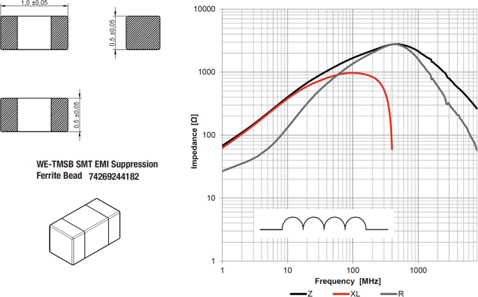
Impedance \(| \underline {Z}|\) [Ω] vs. frequency f [Hz] of the EMI suppression chip ferrite bead Würth Elektronik 74269244182. Courtesy of Würth Elektronik GmbH
-
≈f r . Around f r [Hz], the chip ferrite bead is primarily resistive (\(| \underline {Z}| \approx R\)). The intended use of a ferrite bead for EMI applications is that the component works in this resistive area, where the noise suppression is most effective (converting noise to heat).
-
> f r. For frequencies higher than f r [Hz], the ferrite bead impedance behavior is capacitive due to the parasitic C p [F].


The nonideal behavior of PCB mount ferrite beads comprises the following point:
-
Frequency dependence. As shown in Fig. 11.31, the chip ferrite bead behaves capacitive for frequencies > f r, and the noise suppression for this frequency range is reduced.
-
Temperature influence. The impedance \( \underline {|Z|}\) [Ω] of ferrite beads reduces with increasing temperature T [∘C] (see Fig. 11.32b). Above the Curie temperature (≈ 120…220 ∘C), the magnetic permeability μ r of the ferrite becomes equal 1 (paramagnetic). The ferrite regains its previous permeability when the temperature gets back below the Curie temperature (the effect is reversible).
Fig. 11.32 
Nonideal behavior of ferrite beads. Courtesy of Würth Elektronik GmbH [1]. (a) Impedance \( \underline {|Z|}\) [Ω] vs. DC bias current I [A] of Würth WE-CBF 742861160. (b) Impedance \( \underline {|Z|}\) [Ω] vs. temperature T [∘C] of Würth WE-CBF 742792040
-
DC bias current influence. The impedance \( \underline {|Z|}\) [Ω] of ferrite beads reduces with increasing DC bias current I [A] (see Fig. 11.32a), because the ferrite bead core material moves toward saturation, causing a drop in inductance L [H].

11.6 Common-Mode Chokes
A common-mode choke consists of two coils wound around a common ferromagnetic core (sometimes even more than two coils). The differential signal current flows through one coil and back through the second one (see Fig. 11.34b). Common-mode chokes in EMC are primarily used to block common-mode currents and, therefore, to eliminate unintended radiated electromagnetic emissions.
Figure 11.33d presents the high-frequency equivalent circuit of a common-mode choke, where R s [Ω] represents the ohmic losses, L [H] represents the self-inductance of each coil, M [H] represents the mutual inductance of the coils, R p [Ω] represents the magnetic core losses, C p [F] represents the parasitic capacitance between the turns of the coils, and C 12 [F] represents the parasitic capacitance between the two coils.

Common-mode choke. (a) Common-mode impedances of a common-mode choke. (b) Differential-mode impedances of a common-mode choke. (c) Common-mode choke symbol. (d) High-frequency equivalent circuit of a common-mode choke

Common-mode choke models for common-mode currents I CM vs. differential-mode currents I DM [13]. Parasitic capacitances (C p, C 12) and losses (R s R p) were ignored. (a) I CM = common-mode current. (b) I DM = differential-mode current
When ignoring the parasitic capacitances and the ohmic and magnetic losses, the coil impedances of an ideal common-mode choke can be written as [13]:
where:
-
\( \underline {Z}_1 =\) impedance of common-mode choke coil 1 in [Ω]
-
\( \underline {Z}_2 =\) impedance of common-mode choke coil 2 in [Ω]
-
\( \underline {V}_1 =\) voltage over coil 1 in [V]
-
\( \underline {V}_2 =\) voltage over coil 2 in [V]
-
\( \underline {I}_1 =\) current through coil 1 in [A]
-
\( \underline {I}_2 =\) current through coil 2 in [A]
-
L 1 = self-inductance of coil 1 in [H]
-
L 2 = self-inductance of coil 2 in [H]
-
M 12 = mutual inductance at coil 1 due to coupling with coil 2 in [H]
-
M 21 = mutual inductance at coil 2 due to coupling with coil 1 in [H]
-
ω = 2πf = signal frequency in [rad/s]
If we now assume that the common-mode current I CM [A] splits up equally through both coils of the common-mode choke (I 1CM = I 2CM = I CM∕2) and that the self-inductance of the coils is equal to the mutual inductance (L 1 = L 2 = M 12 = M 21; see Fig. 11.34a), the common-mode impedance of each coil is:
where:
-
\( \underline {Z}_{1CM} =\) ideal common-mode impedance of common-mode choke coil 1 in [Ω]
-
\( \underline {Z}_{2CM} =\) ideal common-mode impedance of common-mode choke coil 2 in [Ω]
-
L = self-inductance of a single coil of the common-mode choke in [H]
-
M = mutual inductance between the coils of the common-mode choke in [H]
-
ω = 2πf = signal frequency in [rad/s]
Equations 11.38 and 11.39 show why common-mode chokes have a high impedance for common-mode currents. On the other hand, an ideal common-mode choke (L 1 = L 2 = M 12 = M 21; see Fig. 11.34b) would not influence the differential-mode current at all:
where:
-
\( \underline {Z}_{1DM} =\) ideal impedance of common-mode choke coil 1 for differential-mode currents in [Ω]
-
\( \underline {Z}_{2DM} =\) ideal impedance of common-mode choke coil 2 for differential-mode currents in [Ω]
-
L = self-inductance of a single coil of the common-mode choke in [H]
-
M = mutual inductance between the coils of the common-mode choke in [H]
-
ω = 2πf = signal frequency in [rad/s]
Figure 11.35 shows the different form factors of common-mode chokes, and Fig. 11.36 presents a typical frequency response of a common-mode choke. Common-mode chokes do influence not only the common-mode signals but also the differential-mode signals (see Fig. 11.36).

Different form factors of common-mode chokes as mains power line filters or low-voltage signal interfaces. Courtesy of Würth Elektronik GmbH

Impedance \(| \underline {Z}|\) [Ω] vs. frequency f [Hz] of the common-mode line filter 744230121 from Würth. Courtesy of Würth Elektronik GmbH
The intentional behavior of common-mode chokes can be summarized like this:
-
Common-Mode current impedance. The magnetic fluxes Φ 1CM [Wb] and Φ 2CM [Wb] through the core caused by the common-mode current I CM [A] through the two coils are added up (see Fig. 11.34a). Ideally, this leads to an inductance L CM [H] that is twice the common-mode choke coil inductance L CM = 2L 1 = 2L 2 and thus leads to high attenuation of common-mode currents.
-
Differential-mode current impedance. The magnetic fluxes Φ 1DM [Wb] and Φ 2DM [Wb] through the core caused by the differential-mode current I DM [A] are subtracted (ideally to zero; see Fig. 11.34b) and do not lead to any saturation of the magnetic core material. This means that even large differential-mode currents do not lead to a saturation of common-mode chokes and thus do not affect the performance of the common-mode noise filtering.
The nonideal (and therefore unintended) behavior of common-mode chokes is summarized here:
-
Frequency dependence. As Fig. 11.36 shows, the common-mode choke influences differential signals at higher frequencies and the common-mode impedance drops. Therefore, it is necessary to check the datasheet if the common-mode choke does not influence the differential-mode signal (which is the useful signal and should therefore not be attenuated or distorted).
-
Temperature influence. The impedance \(| \underline {Z}_{CM}|\) [Ω] of a common-mode choke reduces with increasing temperature T [∘C] until it suddenly drops when the Curie temperature of the magnetic core material is reached. The temperature of common-mode chokes should usually not exceed 125 ∘C or 150 ∘C.
-
Amperage of the differential current. Even though the magnetic flux of the differential current ideally cancels out when flowing through the common-mode choke, it has to be checked that the coils can carry the high differential currents from a thermal standpoint (heating due to ohmic losses).
11.7 Baluns
A balun (a contraction of balanced-unbalanced) is a component that is used to convert between a balanced signal and an unbalanced signal. A balun is a bidirectional component and can be used either way (from balanced to unbalanced and vice versa). There are two main modes of baluns:
-
Voltage balun. The operation of a balun in voltage mode is shown in Fig. 11.37a. Voltage mode is suitable for impedance matching applications [11] and applications that require galvanic isolation.
Fig. 11.37 
Baluns. (a) Balun in voltage mode. (b) Autotransformer baluns are electrically non-isolating and operate with only one winding. (c) Balun in current mode
-
Current balun. The current mode operation of a balun is shown in Fig. 11.37c. In current mode operation, it adds impedance to unwanted common-mode current and helps to eliminate them effectively [11]).

In addition to a distinction between voltage and current baluns, there is also a distinction between isolation transformers (Fig. 11.37a) and autotransformers (Fig. 11.37b). Typical balun applications are:
-
RF transceiver to antenna interface. A balun can act as an interface converter between a single-ended RF transceiver and a balanced antenna.
-
Unbalanced to balanced interface. A balun can act as an interface between an unbalanced (microstrip line, single-ended signal) and a balanced transmission line (twisted-pair, differential signal) and vice versa (Fig. 11.38).
Fig. 11.38 
10BASE-T1 and 100BASE-T1 Single Pair Ethernet (SPE) interface with galvanic isolation of 1.5 kV and balun WE-STST 74930000 from Würth. Courtesy of Würth Elektronik GmbH
-
Impedance matching. A balun can also be used to transform between different system impedances. In other words, a balun is an impedance matching component.

The applications and use cases for baluns are very broad. Therefore, it is difficult to give a conclusive set of properties to watch out for. The first thing to decide is if a voltage or a current balun or an autotransformer balun with only one coil is needed. If you are unsure which type of balun you need, you could look for an application note that describes your application best and start with the solution described there.
11.8 Clamping Devices
Voltage clamping devices —like varistors (Sect. 11.8.1) and TVS diodes (Sect. 11.8.2)—commonly block the current flow up to a specified voltage. Once the voltage reaches that clamping voltage, the voltage across the voltage clamping device does not increase anymore. In other words, the voltage is clamped. Voltage clamping devices are commonly used to protect circuits from transient pulses like:
-
ESD. IEC 61000-4-2, 1/60 nsec-pulses of 1 nsec rise-time by 60 nsec duration.
-
Bursts (EFTs). IEC 61000-4-4, 5/50 nsec-pulses of 5 nsec rise-time by 50 nsec duration.
-
Surges. IEC 61000-4-5, 8/20 µsec-pulses of 8 µsec rise-time by 20 µsec duration.
Figure 11.46 shows how a voltage clamping device limits the transient voltage across its pins.
11.8.1 Varistors
Varistors are voltage-dependent resistors (VDR), and they are typically used as overvoltage protection devices against bursts (EFTs) and surges, which arrive at the victim via the public mains supply or the DC supply port. Varistors belong to the category of clamping devices.
The high-frequency equivalent circuit for varistors is presented in Fig. 11.39. The series inductance L s [H] represents the varistor’s terminal inductance (approximately 1 nH/mm), the series resistor R s [Ω] represents the varistor’s terminal resistance (a few [mΩ]), the parallel capacitance C p [F] represents the intergranular capacitance (10 pF up to 10 nF), the parallel resistor R p [Ω] represents the intergranular resistance (several [MΩ]), and finally R V ar [Ω] represents the ideal varistor (0 Ω to ∞ Ω) (Fig. 11.40).

Equivalent circuit of a varistor [5]

Different form factors of varistors. Courtesy of Würth Elektronik GmbH

Varistor (VDR). (a) Schematic symbol of varistors. The letter U is often used instead of the letter V. (b) Current I [A] vs. voltage V [V] of ZnO and SiC varistors. ZnO VDRs belong to the category of metal oxide varistors (MOV) and are the most common.
Figure 11.41b presents a varistor’s nonlinear and bidirectional current-voltage characteristic, and Fig. 11.42 presents extracted data from a varistor’s datasheet. At the breakdown voltage V BR [V] or varistor voltage V V ar [V], the varistor changes its state from insulating to conducting. Usually, the breakdown voltage is specified for 1 mA DC current. Ideally, a VDR would block every current as long as the voltage across the VDR is smaller than the breakdown voltage V BR [V], and as soon it is larger than V BR [V], the voltage would not increase and an infinite amount of current could flow through the VDR.

Varistor 820442711E from Würth for 230 VAC applications. Courtesy of Würth Elektronik GmbH

TVS diodes. (a) Different form factors of TVS diodes. Courtesy of Würth Elektronik GmbH. (b) Left: unidirectional TVS diode. Right: bidirectional TVS diode
Unfortunately, we do not live in an ideal world, and VDRs have some points to be considered when using them in a design:
-
Operating voltage. Up to this voltage, the varistor does not conduct. The operating voltage in the datasheet specifies the maximum operating voltage (consider power supply tolerances when calculating the maximum operating voltage).
-
Breakdown voltage. The breakdown voltage V BR [V] specifies typically the voltage where the DC current through the varistor is 1 mA. When a voltage is applied, which exceeds V BR [V], the junctions experience an avalanche breakdown, and a large current can flow.
-
Energy absorption. Depending on the case size, the energy absorption varies from 0.01 J (SMT 0402) up to 10 kJ (chassis mount). Most varistors can absorb 5/50 nsec-burst-pulses and/or 8/20 µsec-surge pulses (take care which immunity level you need for your product: 1, 2, 3, or 4). Figure 11.40 shows different form factors and case sizes of VDRs.
-
Response time. Most varistors have a response time that exceeds > 25 nsec [6], which makes them too slow for ESD protection (IEC 61000-4-2, 1/60 nsec-pulses). VDRs with a fast response time of < 1 nsec—which is fast enough to protect against ESD-pulses—usually have the downside that they cannot absorb enough energy for surge pulses.
-
Clamping voltage. The clamping voltage V clamp [V] describes the voltage across the VDR for a certain pulse (rise-time) and current. Unfortunately, V clamp is usually much higher than the breakdown voltage V BR [V]. Therefore, care must be taken that the circuit to be protected can withstand V clamp [V] without any damage.
-
Capacitance. The parallel capacitance C p [F] of varistors is much higher than the capacitance of TVS diodes or gas discharge tubes. C p [F] is usually in the range of 10 pF up to 10 nF [6] and, therefore, too high for high-speed signal interfaces. However, in the case of the protection of AC or DC power inputs, the parallel capacitance C p is very welcome and can be used to replace filter capacitors.
-
Leakage current. The leakage current depends on the voltage which is applied across the VDR, and it is usually in the range of 1 µA to <1 mA. The leakage current can be extracted from the current-to-voltage characteristic curve for any given voltage (see Fig. 11.42).
-
Aging. As shown in Fig. 11.42, VDRs show an aging effect based on the number of current pulses they experience.
11.8.2 TVS Diodes
Transient-voltage-suppression diodes (TVS diodes) are typically used as overvoltage protection devices against ESD pulses, bursts (EFTs), and surges (if the current through the diode is limited). TVS diodes belong to the category of clamping devices. Figure 11.43a presents different form factors of TVS diodes.

Current I [A] vs. voltage V [V], a bidirectional TVS diode
Compared to varistors, TVS diodes have a shorter response time and a lower clamping voltage V clmap [V] (for the same breakdown voltage V BR [V]). On the other side, TVS diodes do endure less pulse current I PP [A] compared to varistors. TVS diodes are available in two configurations:
-
Unidirectional. Forward operation: normal silicon diode with V f ≈0.7 V. Reverse operation: transient protection with defined breakdown voltage V BR [V].
-
Bidirectional. Both directions can be used for transient protection with defined breakdown voltage V BR [V].
Figure 11.44 presents a typical current vs. voltage curve of a bidirectional TVS diode. The most essential parameters of TVS a diode are:
-
Reverse standoff voltage, reverse working voltage. Up to the reverse working voltage V RWM [V], the suppressor diode does not conduct any significant amount. V RWM [V] must always be greater than the maximum operating voltage (consider all the tolerances of the signal’s amplitude).
Fig. 11.45 
TVS diode 824012823 from Würth for high-speed interfaces like USB 3.1 (10 GB/s) or HDMI 2.0. Courtesy of Würth Elektronik GmbH
-
Breakdown voltage. At the breakdown voltage V BR [V], the TVS diode starts to conduct and the diode changes to the conductive state.
-
Clamping voltage. At the clamping voltage V clamp [V], the suppressor diode carries the maximum current I PP [A]. Therefore, care must be taken that the circuit to be protected can withstand V clamp [V] without any damage.
-
Peak pulse current. At the peak pulse current I PP [A], the TVS diode gets the maximum energy that a short electrical pulse can convert into heat in the suppressor diode without damaging it.
-
Leakage current. The leakage current is the current that flows in the reverse direction through the suppressor diode at a given voltage.
-
Parasitic parallel capacitance. The parasitic parallel capacitance of the diode could lead to bad signal integrity in the case of high-speed signal interfaces.
-
Insertion loss IL. TVS diodes designed for high-speed interfaces often specify the insertion loss IL [dB] of the TVS diodes in their datasheets (see Fig. 11.45).
Fig. 11.46 
Voltage pulse response of voltage clamping and crowbar devices


11.9 Crowbar Devices
Crowbar devices commonly block the current flow up to a specific voltage. Once that voltage is exceeded, the crowbar device changes suddenly into a low impedance state, the voltage across the crowbar device gets low, and the current through the crowbar device increases and is only limited by the external circuit. After that, when the current through the crowbar device falls below a certain threshold, the crowbar device resets itself. Examples of crowbar devices are TVS thyristors (see Fig. 11.47b) and gas discharge tubes (see Fig. 11.47c). Crowbar devices are mainly used to protect circuits from high-energy transient pulses like:
-
Surges. IEC 61000-4-5, 8/20 µsec-pulses of 8 µsec rise-time by 20 µsec duration.
Fig. 11.47 
Schematic symbols of typical crowbar devices. (a) Thyristor symbol. (b) Symbols of dedicated TVS thyristors, also called thyristor surge protection device (TSPD). (c) Symbols of a gas discharge tubes (GDT) with two electrodes and three electrodes
-
EMP transients. Electromagnetic pulse (EMP) transients are transients generated by EMPs that are produced, e.g., by detonations of nuclear explosive.

Compared to voltage clamping devices (see Sect. 11.8), the crowbar devices can handle much more energy, but the downside is that they do not turn on as fast as voltage clamping devices. Figure 11.46 compares the principles of voltage clamping vs. crowbar behavior (Fig. 11.47).
We do not go further into detail about crowbar devices because for many products on the market, the presented clamping devices—like varistors and TVS diodes, in combination with other passive filter components like capacitors,—are most practical and economical to use. However, gas discharge tubes are very popular for lightning protection of antennas and telecommunication products.
References
Application Note - Behind the Magic of High Frequency SMT Chip Bead Ferrites. Würth Elektronik eiSos GmbH & Co. KG. Oct. 21, 2020.
Constantine A. Balanis. Antenna Theory - Analysis and Design. 3rd edition. John Wiley & Sons Inc., 2005.
Eric Bogatin. Signal and Power Integrity - Simplified. 3rd edition. Prentice Hall Signal Integrity Library, 2018.
Chris Bowick. RF Circuit Design. Newens, 1982.
Dr. Thomas Brander et al. Trilogy of Magnetics. 5th edition. Würth Elektronik eiSos GmbH & Co. KG, 2018.
ESD and Surge protection on the PCB. Würth Elektronik eiSos GmbH & Co. KG. 2019.
Fixed capacitors for use in electronic equipment - Part 14: Sectional specification - Fixed capacitors for electromagnetic interference suppression and connection to the supply mains. International Electrotechnical Commission (IEC). 2013.
Würth Elektronik Group. REDEXPERT - Online platform for electronic component selection and simulation. June 4, 2021. https://redexpert.we-online.com/.
Dr. Howard Johnson and Martin Graham. High-Speed Signal Propagation: Advanced Black Magic. Prentice Hall, 2003.
KEMET. Here’s What Makes MLCC Dielectrics Different. June 4, 2021. https://ec.kemet.com/blog/mlcc-dielectric-differences/.
Mini-Circuits. Demystifying Transformers: Baluns and Ununs. July 9, 2020. https://blog.minicircuits.com/demystifying-transformers-baluns-and-ununs/.
Henry W. Ott. Electromagnetic Compatibility Engineering. John Wiley & Sons Inc., Sept. 11, 2009.
Clayton R. Paul. Introduction to electromagnetic compatibility. 2nd edition. John Wiley & Sons Inc., 2008.
SR Series: Surge Resistors for PCB Mounting. HVR International. 2020.
Inc. Vishay Intertechnology. Pulse Handling Capabilities of Vishay Dale Wirewound Resistors. Sept. 1, 2021. https://www.digikey.com/en/articles/pulse-handling-capabilities-of-vishay-dale-wirewound-resistors.
Brian C. Wadell. Transmission line design handbook. Artech House Inc., 1991.
Author information
Authors and Affiliations
Rights and permissions
Open Access This chapter is licensed under the terms of the Creative Commons Attribution 4.0 International License (http://creativecommons.org/licenses/by/4.0/), which permits use, sharing, adaptation, distribution and reproduction in any medium or format, as long as you give appropriate credit to the original author(s) and the source, provide a link to the Creative Commons license and indicate if changes were made.
The images or other third party material in this chapter are included in the chapter's Creative Commons license, unless indicated otherwise in a credit line to the material. If material is not included in the chapter's Creative Commons license and your intended use is not permitted by statutory regulation or exceeds the permitted use, you will need to obtain permission directly from the copyright holder.
Copyright information
© 2023 The Author(s)
About this chapter

Cite this chapter
Keller, R.B. (2023). Components. In: Design for Electromagnetic Compatibility--In a Nutshell. Springer, Cham. https://doi.org/10.1007/978-3-031-14186-7_11
Download citation
DOI: https://doi.org/10.1007/978-3-031-14186-7_11
Published:
Publisher Name: Springer, Cham
Print ISBN: 978-3-031-14185-0
Online ISBN: 978-3-031-14186-7
eBook Packages: EngineeringEngineering (R0)