
Abstract
The field-effect transistor or FET is a three-terminal semiconductor device that controls an electric current by an electric field. The FET actually pre-dates the BJT as the first patent was granted for such a device in 1928. Its impact on industry however was felt only about a decade after the development of the transistor in 1948. The FET is a unipolar device having only one p-n junction, and it differs from the BJT in several important respects, the main one being the FET’s inherently high input impedance. There are two types of FETS: the junction gate FET (JFET or JUGFET) and the metal oxide semiconductor FET or MOSFET. The MOSFET, sometimes called the insulated gate FET or IGFET, itself comes in two versions: the depletion MOSFET and the enhancement MOSFET. Because of a difference in construction, the MOSFET has a higher input impedance than the JFET. The FET like the BJT can provide amplification of a signal and operate as a switch. It is important in many applications and forms the subject of this chapter. At the end of the chapter, the student will be able to:
Access this chapter
Tax calculation will be finalised at checkout
Purchases are for personal use only
Bibliography
R.L. Boylestad, L. Nashelsky, Electronic Devices and Circuit Theory, 11th edn. (Pearson Education, New Jersey, 2013)
J. Eimbinder, FET Applications Handbook, 2nd edn. (Tab Books, Pasadena, 1970)
F.G. Rayer, 50 (FET) Field Effect Transistor Projects (Babani Press, London, 1977)
Author information
Authors and Affiliations
Problems
Problems
-
1.
Briefly explain the following:
-
(a)
The high input impedance of a JFET
-
(b)
The high input impedance of a MOSFET
-
(c)
The main difference between enhancement and depletion mode MOSFETS
-
(d)
Pinch-off in a JFET
-
(e)
The difference between n-channel and p-channel JFETS
-
(f)
The main similarity between a BJT and an enhancement-type MOSFET
-
(g)
The main similarity between a JFET and a depletion-type MOSFET
-
(a)
-
2.
A JFET has a signal voltage of 0.75Vpk value applied to its gate relative to its source. The drain current varies by ±1.5 mA about its quiescent value. Calculate gm.
-
3.
An n-channel JFET has IDSS = 6 mA and VP = −5 V. For a drain current of 4 mA, determine gm using Shockley’s equation. If this JFET is used in a common source amplifier with its source grounded for signals and drain resistance RL = 10 k , determine the voltage gain from gate to drain.
-
4.
Using fixed-bias, bias a n-channel JFET for a drain current of 3 mA using a device having IDSS = 7 mA and VP = − 4 V. Use VDD = 14 V and choose RL for maximum symmetrical swing.
-
5.
Bias a p-channel JFET for a drain current of 2 mA using fixed-bias. For the FET, IDSS = 12 mA and VP = +5 V. Use VDD = −18 V and select RL for maximum symmetrical swing.
-
6.
Using the FET of problem 4 above, find RS to replace the fixed-bias voltage source VGG.
-
7.
Using Shockley’s equation \( {I}_D={I}_{DSS}{\left(1-\frac{V_{GS}}{V_P}\right)}^2 \) and a 26 volt supply, design a common source amplifier based on self-bias, using an n-channel JFET having a pinch-off voltage of −2.5 volts and IDSS = 5 mA. Use a 3 mA quiescent current. Use \( {g}_m=-2\frac{\sqrt{I_D{I}_{DSS}}}{V_P} \) to calculate the voltage gain of your circuit.
-
8.
Using an n-channel JFET having IDSS = 3 mA and VP = − 5.5 volts, bias the device using voltage divider biasing for a drain current of 2.5 mA. Design for a maximum symmetrical swing with VDD = 18 volts.
-
9.
State the advantages and disadvantages of self-bias as compared with voltage divider bias in JFETS.
-
10.
For the self-biased common source amplifier in problem 7, re-design the system to use a bipolar supply of ±15 V, returning RS to the negative supply voltage.
-
11.
Using Shockley’s equation \( {I}_D={I}_{DSS}{\left(1-\frac{V_{GS}}{V_P}\right)}^2 \) and a 27 volt supply, design a common source amplifier using an p-channel JFET having a pinch-off voltage of +4 volts and IDSS = 6 mA. Use a 1 mA quiescent current and fixed-bias. Noting \( {g}_m=-2\frac{\sqrt{I_D{I}_{DSS}}}{V_P} \), determine the voltage gain of your circuit.
-
12.
Using Shockley’s equation \( {I}_D={I}_{DSS}{\left(1-\frac{V_{GS}}{V_P}\right)}^2 \) and an 18 volt supply, design a common source amplifier using an n-channel JFET having a pinch-off voltage of −3 volts and IDSS = 4 mA. Use voltage divider bias and a 2 mA quiescent current. Explain the functions of the input gate resistor and the source resistor.
-
13.
Using Shockley’s equation and a 24 volt supply, design a common source amplifier using an n-channel depletion MOSFET having a pinch-off voltage of −4 volts and IDSS = 5 mA. Use a 5 mA quiescent current and self-bias. Calculate the voltage gain of your circuit using \( {g}_m=-2\frac{\sqrt{I_D{I}_{DSS}}}{V_P} \).
-
14.
For the fixed-bias common source amplifier in problem 13, re-design the system to use a bipolar supply of ±22 V and return RS to the negative supply voltage instead of ground.
-
15.
Determine the drain current in the circuit shown in Fig. 3.64. if the quiescent gate-source voltage for the JFET is −2.8 V
Fig. 3.64 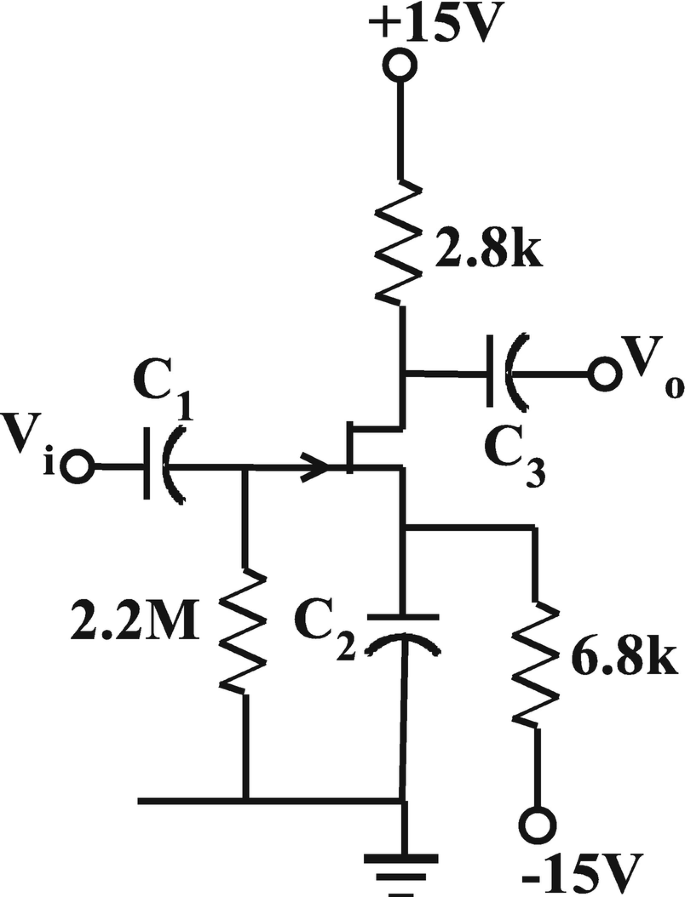
Circuit for Question 15
.
-
16.
Design a common drain amplifier using an n-channel JFET having IDSS = 4.1 mA and VP = − 5.3 V and voltage divider biasing. Design for a maximum symmetrical swing with VDD = 27 V.
-
17.
Design a source follower circuit using a p-channel JFET with IDSS = 8 mA, VP = + 2.3 V and a −12 V supply.
-
18.
For the common drain amplifier in problem 16, re-design the system to use a bipolar supply of ±18 V and return RS to the negative supply voltage instead of ground.
-
19.
Design a common gate amplifier using an n-channel JFET having IDSS = 3.2 mA and VP = − 1.9 V. Design for a maximum symmetrical swing with VDD = 18 V.
-
20.
Using self-bias, design a biasing network for a common source n-channel depletion-type MOSFET having IDSS = 2.9 mA and VP = − 4.7 V. Design for maximum symmetrical swing.
-
21.
Using an n-channel depletion MOSFET having IDSS = 3.7 mA and VP = − 3.9 V, bias the device for common source operation using voltage divider biasing and a drain current of 3 mA. Design for a maximum symmetrical swing with VDD = 16 V.
-
22.
Repeat the design in problem 21 using a p-channel depletion MOSFET having IDSS = 4.1 mA and VP = + 4.7 V.
-
23.
Design a common drain amplifier using an n-channel depletion MOSFET having IDSS = 5.9 mA and VP = − 6.1 V. Design for maximum symmetrical swing with VDD = 32 V.
-
24.
Design a common gate amplifier using an n-channel depletion MOSFET with IDSS = 1.3 mA and VP = − 2.9 V. Design for maximum symmetrical swing using a 14 V supply.
-
25.
Using the circuit shown in Fig. 3.65, design a feedback biasing network for an enhancement-type MOSFET having VT = 2.7 V, IDon = 5 mA and VGSon = 7 V. Use VDD = 15 V
Fig. 3.65 
Circuit for Question 25
.


-
26.
Design a feedback biasing network for a common source enhancement-type p-channel MOSFET having VGST = 2.5 V, IDon = 4 mA and VGSon = 7 V. Use VDD = 25 V.
-
27.
Using the configuration in Fig. 3.66, design a modified feedback biasing network for a common source enhancement-type MOSFET having VT = 3.3 V, IDon = 6.4 mA and VGSon = 5.3 V. The supply voltage is VDD = 12 V
Fig. 3.66 
Circuit for Question 27
.

-
28.
Using the configuration in Fig. 3.67, design a voltage divider-biased common source amplifier using an enhancement-type MOSFET having VT = 2.4 V and k = 0.07 mA/V2, and use VDD = 22 V
Fig. 3.67 
Circuit for Question 28
.

-
29.
Using the configuration in Fig. 3.49, design a voltage divider-biased common drain amplifier using an enhancement-type n-channel MOSFET having VT = 2.4 V and k = 0.29 mA/V2, and use VDD = 25 V.
-
30.
Using the configuration in Fig. 3.50, design a voltage divider-biased common gate amplifier using an enhancement-type MOSFET having VT = 2.1 V and k = 0.05 mA/V2, and use VDD = 30 V.
Rights and permissions
Copyright information
© 2021 Springer Nature Switzerland AG
About this chapter

Cite this chapter
Gift, S.J.G., Maundy, B. (2021). Field-Effect Transistor. In: Electronic Circuit Design and Application. Springer, Cham. https://doi.org/10.1007/978-3-030-46989-4_3
Download citation
DOI: https://doi.org/10.1007/978-3-030-46989-4_3
Published:
Publisher Name: Springer, Cham
Print ISBN: 978-3-030-46988-7
Online ISBN: 978-3-030-46989-4
eBook Packages: EngineeringEngineering (R0)