
Abstract
Integrated components that do not amplify current or voltage signals belong to a family of devices referred to as passive components. This includes resistors, capacitors, varactors, and inductors. This chapter describes passive components that can be integrated in a CMOS technology. The design and characteristics of different types of resistors, capacitors, varactors, and spiral inductors are described, followed by simple examples of their applications in analog circuits. Passive components, in particular capacitor and resistors, occupy a substantial area of the chip (Fig. 1.12). They should be optimized by minimizing the area while maintaining the desired electrical properties.
Access this chapter
Tax calculation will be finalised at checkout
Purchases are for personal use only
References
K. Kato, T. Ono, Y. Amemiya, Electrical trimming of polycrystalline silicon resistors and its application to analog ICs. IEEE Trans. Electron Dev 27(11), 2194–2195 (1979)
W.A. Lane, G.T. Wrixon, The design of thin-film polysilicon resistors for analog applications. IEEE Trans. Electron Dev. 36(4), 738–744 (1989)
F. Hegner, The industrial production of high-quality nickel-chromium resistors with controlled temperature coefficient of resistance. Thin Solid Films 57(2), 359–362 (1979)
G. Nocerino, K.E. Singer, The electrical and compositional structure of thin Ni-Cr films. Thin Solid Films 57(2), 343–348 (1979)
M.A. Bayne, Al-doped Ni-Cr for temperature coefficient of resistance control in hybrid thin-film resistors. J. Vac. Sci. Technol. A4(6), 3142–3145 (1986)
F. Wu, A.W. McLaurin, K.E. Henson, D.G. Managhan, S.L. Thomasson, The effects on the process parameters on the electrical and microstructure characteristics of the CrSi thin resistor films: Part I. Thin Solid Films 332(1–2), 418–422 (1998)
D. Nachrodt, U. Pachen, A. Ten Have, H. Vogt, Ti/Ni(80%)Cr(20%) thin-film resistor with near zero temperature coefficient of resistance for integration in a standard CMOS process. IEEE Electron Dev. Lett. 29(3), 212–214 (2008)
P. Zurcher, P. Alluri, P. Chu, A. Duvallet, C. Happ, R. Henderson, J. Mendonca, M. Kim, M. Petras, M. Raymond, T. Remmel, D. Roberts, B. Steimle, J. Sipanuk, S. Straub, T. Sparks, M. Tarabbia, H. Thibieroz, M. Miller, Integration of thin-film MIM capacitors and resistors into copper metallization based RF-CMOS and BiCMOS technologies. IEEE IEDM Tech. Digest, 153–156 (2000)
R.W. Berry, P.M. Hall, M.T. Harris, Thin Film Technology (Van Nostrand, 1968)
S.M. Sze, Physics of Semiconductor Devices (John Wiley & Sons, 1981), p. 43
M.G. Holland, Phonon scattering in semiconductors from thermal conductivity studies. Phys. Rev. 134, A471 (1964)
B.H. Armstrong, The physics of SiO2 and its interfaces, in Thermal Conductivity in SiO2, ed. by S. T. Pantelides, (Pargamon Press, New York, 1978)
C.Y. Ho, R.W. Powell, P.E. Liley, Thermal Conductivity of the Elements, a Comprehensive Review (American Chemical Society and American Institute of Physics, New York, 1975)
T.I. Kamins, Hall mobility in chemically deposited polycrystalline silicon. J. Appl. Phys. 42(11), 4357–4365 (1971)
J.Y. Seto, The electrical properties of polycrystalline silicon films. J. Appl. Phys. 46(12), 5247–5254 (1975)
H.M. Chuang, S.F. Tsai, K.B. Thei, S.F. Tsai, W.C. Li, Temperature-dependent characteristics of diffused and polysilicon resistors. IEEE Trans. Electron. Dev. 50(5), 1413–1415 (2003)
D.N. Kouvatsos, A.T. Voutsas, M.K. Hatalis, High-performance thin-film transistors in large grain size polysilicon deposited by thermal decomposition of disilane. IEEE Trans. Electron Dev. 43(9), 1399–1406 (1996)
M. Koda, Y. Shida, J. Kawaguchi, Y. Kaneko, Improving gate oxide integrity in p+pMOSFET by using large grain size polysilicon gate. IEEE IEDM Tech. Digest, 471–474 (1993)
N.C.-C. Lu, L. Gerzberg, C.-Y. Lu, J.D. Meindl, Modeling and optimization of monolithic polycrystalline silicon resistors. IEEE Trans. Electron Dev. ED-28(7), 818–830 (1981)
T.A. Carbone, P. Plourde, E. Karagiannis, Correlation of ellipsometric volume fraction to polysilicon grain size from transmission electron microscopy. IEEE/SEMI ASMC, 359–367 (1999)
M.M. Mandurah, K.C. Saraswat, T.I. Kamins, Phosphorus doping of low pressure chemically vapor-deposited silicon films. J. Electrochem. Soc. 126(8), 1019–1023 (1979)
N.C.C. Lu, L. Gerzberg, J.D. Meindl, A quantitative model of the effect of grain size on the resistivity of polycrystalline silicon resistors. Electron Dev. Lett. EDL-1(3), 38–41 (1980)
M.E. Cowher, T.O. Sedgwick, Chemical vapor deposited polycrystalline silicon. J. Electrochem. Soc. 119(11), 1565–1570 (1972)
A.L. Fripp, Dependence of resistivity on the doping level of polycrystalline silicon. J. Appl. Phys. 46(3), 1240–1244 (1975)
P. Rai-Choudhury, P.L. Hower, Growth and characterization of polycrystalline silicon. J. Electrochem. Soc. 120(12), 1761–1766 (1971)
G. Baccarani, B. Riccò, Transport properties of polycrystalline silicon films. J. Appl. Phys. 49(11), 5565–5570 (1978)
M. Nakabayshi, M. Ikegami, T. Daikoku, Influence of hydrogen on electrical characteristics of poly-Si resistor. Jpn. J. Appl. Phys. 32(Part 1 (9A)), 3734–3738 (1993)
M.M. Mandurah, K. Saraswat, T.I. Kamins, A model for conduction in polycrystalline silicon – Part II: Comparison of Theory and experiment. IEEE Trans. Electron Dev. ED-28(10) (1981)
W.-C. Liu, K.-B. Thei, H.-M. Chuang, K.-Y. Lin, C.-C. Cheng, Y.-S. Ho, C.-Y. Su, S.-C. Wong, C.-H. Lin, C.-H. Dias, Characterization of polysilicon resistors in sub-0.25μm CMOS ULSI applications. IEEE Electron Dev. Lett. 22(7), 318–320 (2001)
L.J. Van der Pauw, A method of measuring specific resistivity and Hall effect of disc of arbitrary shape. Phillips Res. Reports 13, 1–9 (1958)
C.M. Osburn, J.Y. Tsai, Q.F. Wang, J. Rose, A. Cowen, Predict 1.6: Modeling of metal silicide processes. J. Electrochem. Soc. 140(12), 3660–3670 (1993)
M.S. Raman, T. Kifle, E. Bhattacharya, K.N. Bhat, Physical model for the resistivity and temperature coefficient of resistivity in heavily doped Polysilicon. IEEE Trans. Electron Dev. 53(8), 2006 (1885-1892)
D.W. Lee, T.M. Roh, H.S. Park, J. Kim, J.G. Koo, D.Y. Kim, Fabrication technology of polysilicon resistors using novel mixed process for analogue CMOS application. IEEE Electronic Lett. 35(7), 803–804 (1999)
W. Tatinian, E. Simoen, N. Ouassif, B. Desoete, R. Gillon, P. Pannier, Self-heating based model for polysilicon resistors. IEEE Midwest Symp. Circuits and Systems, MWSCAS, Tech. Digest 3, 1337–1339 (2004)
P. Steinmann, E. Beach, W. Meinel, A. Chatterjee, D. Weiser, R. Bucksch, W. Tang, Simple analytical model of the thermal resistance of resistors in integrated circuits. IEEE Trans. Electron Dev. 57(5), 1029–1036 (2010)
N.C.C. Lu, L. Gerzberg, C.Y. Lu, D. Meindl, A conduction model for semiconductor grain boundary- semiconductor barriers in polycrystalline silicon films. IEEE Trans. Electron Dev. ED-30, 137–149 (1983)
Y. Amemiya, T. Ono, K. Kato, Electrical trimming of heavily doped polycrystalline silicon resistors. IEEE ED-26(11), 1138–1142 (1979)
S. Das, S.K. Lahiri, Electrical trimming of ion-beam sputtered polysilicon resistors by high current pulses. IEEE Trans. Electron Dev. 41(8), 1429–1435 (1994)
K. Kato, T. Ono, Y. Amemiya, A physical mechanism of current-induced resistance decrease in heavily doped polysilicon resistors. IEEE Trasn. Electron Dev. ED-29(8), 1156–1161 (1982)
K. Kato, T. Ono, Y. Amemiya, A monolithic 14 bit D/a converter fabricated with a new trimming technique (DOT). IEEE J. Solid State Circuits 19(5), 802–807 (1984)
M.I. Elmasry, Capacitance calculations in MOSFET VLSI. IEEE Electron Dev. Lett. EDL-3(1), 6–7 (1982)
R. Shrivastava, K. Fitzpatrick, A simple model for the overlap capacitance of a VLSI MOS device. IEEE Trans. Electron Dev. ED-29(12), 1982 (1870-1875)
K. Suzuki, Parasitic capacitance of sub-micrometer MOSFETs. IEEE Trans. Electron. Dev. 46(9), 1999 (1895-1900)
A. Ito, Modeling of voltage-dependent diffused resistors. IEEE Trasn. Electron Dev. 44(12), 2300–2302 (1997)
C.C. McAndrew, T. Bettinger, Robust parameter extraction for the R3 nonlinear resistor model for diffused and poly resistors. IEEE Trans. Semiconductor Manufacturing 25(4), 255–263 (2012)
P. Steinmann, S.M. Stuart, R. Higgins, Controlling the TCR of thin film resistors. Euro. Dev. Res. Conf., 451–453 (2000)
C.A. Neugebauer, M.B. Webb, Electrical conduction mechanism in ultrathin, evaporated metal films. J. Appl. Phys. 33, 74–82 (1962)
J.R. Sambles, T.W. Preist, The effects of surface scattering upon resistivity. J. Phys. F 12, 1982 (1971-1987)
P. Fehlhaber, Laser trimming of SiCr thin-film resistors. IEEE IEDM Tech. Digest, 9–10 (1969)
R.H. Wagner, Functional laser trimming: An overview. Laser Processing of Semiconductors and Hybrids, SPIE Proceedings 611, 8–17 (1986)
M.J. Mueller, W. Mickanin, Functional laser trimming of thin film resistors on silicon IC. Laser Processing of Semiconductors and Hybrids, SPIE Proceedings 611, 70–83 (1986)
A.C. Adams, in Dielectric and Polysilicon Film Deposition, VLSI Technology, ed. by S. M. Sze, 2nd edn., (McGraw-Hill, 1988), pp. 259–263
J.L. McCreary, Matching properties, and voltage and temperature dependence of MOS capacitors. IEEE J. Solid State Circuits SC-16(6), 608–616 (1981)
J.W. Fattaruso, M. De Wit, G. Warwar, K.S. Tan, R.K. Hester, The effect of dielectric relaxation on charge-redistribution a/D converters. IEEE J. Solid State Circuits 25(6), 1550–1561 (1990)
K. Hyyppä, Dielectric absorption in memory capacitors. IEEE Trans. Instrum. Meas. 21(1), 53–56 (1972)
J.C. Kuenen, G.C.M. Meijer, Measurement of dielectric absorption of capacitors and analysis of its effects on VCO. IEEE Trans. Instrum. Meas. 45(1), 89–97 (1996)
C. Iorga, Compartmental analysis of dielectric absorption in capacitors. IEEE Trans. Dielectrics 7(2), 187–192 (2000)
T.I. Liou, C.S. Teng, N+−poly-to-n+−silicon capacitor structure for single poly analog CMOS and BiCMOS. IEEE Trans. Electron Dev. 36(9), 1620–1628 (1989)
S.A.S. Onge, S.G. Franz, A.F. Puttlitz, A. Kalinoski, B.E. Johnson, B. El-Kareh, Design pf precision capacitors for analog applications. IEEE Components, Hybrids, and Manufacturing Technology 15(6), 1064–1071 (1992)
P.K. Hurley, L. Wall, A. Mathewson, Double Polysilicon capacitors in 1 μm analogue CMOS technology. European Solid-State Device Research Conference, ESSDERC, 569–572 (1993)
S.G. Lee, J.T. Lee, J.K. Choi, High-Q poly-to-poly capacitor for RF integrated circuits. Electronics Lett. 37(1), 25–26 (2001)
C. Kaya, H. Trigelar, J. Paterson, M. De Wit, J. Fattsruso, R. Hester, S. Kiriaki, K.S. Tan, F. Tsay, Polycide/metal capacitors for high precision analog a/D converters. IEEE IEDM Tech. Digest, 782–785 (1988)
J.A. Babcock, S.G. Balster, A. Pinto, C. Dirnecker, P. Steinmann, R. Jumpertz, B. El-Kareh, Analog characteristics of metal-insulator-metal capacitors using PECVD nitride dielectrics. IEEE Trans. Electron Dev. 22(5), 230–232 (2001)
C.H. Ng, C.S. Ho, S.F.S. Chu, S.C. Sun, MIM capacitor integration for mixed-signal/RF applications. IEEE Trans. Electron Dev. 52(7), 1399–1409 (2005)
K. Stein, J. Kocis, G. Hueckel, E. Eid, T. Bartush, R. Groves, N. Greco, D. Harame, T. Tewksbury, High reliability metal insulator metal capacitors for silicon germanium analog applications. IEEE BCTM Tech. Digest, 191–194 (2007)
C.N. Ng, K.W. Chew, S.F. Chu, Characterization and comparison of PECVD silicon nitride and silicon Oxynitride dielectric for MIM capacitors. IEEE Electron Dev. Lett. 24(8), 506–508 (2003)
T. Yoshitomi, Y. Ebuchi, H. Kimijima, T. Ohguro, E. Morifuji, H.S. Momose, K. Kasai, K. Ishimaru, F. Matruoka, Y. Katsumata, M. Kinogawa, H. Iwai, High performance MIM capacitor for RF BiCMOS/CMOS LSIs. IEEE BCTM Tech. Digest, 133–136 (1999)
M. Armacost, A. Augustin, P. Felsner, Y. Feng, G. Friese, J. Heidenreich, G. Hueckel, O. Prigge, K. Stein, A high reliability metal insulator metal capacitor for 0.18 μm copper technology. IEEE IEDM Tech. Digest, 157–160 (2000)
R. Liu, C.Y. Lin, E. Harris, S. Merchant, S.W. Downey, G. Weber, N.A. Ciampa, W.T. Warren, Y.C. Lai, M.D. Morris, J.E. Bowe, J.F. Miner, J. Frackoviak, W. Mansfield, D. Barr, R. Keller, C.P. Chang, C.S. Pai, S.N. Rogers, R. Gregor, Single mask metal-insulator-metal (MIM) capacitor with copper damascene metallization for sub-0.18mm mixed mode signal and system-on-a-chip (SoC) applications. IEEE IITC, 111–113 (2000)
R. Mahnkopf, K.H. Allers, M. Armacost, A. Augustin, J. Barth, G. Brase, R. Busch, E. Demm, G. Dietz, B. Flietner, G. Friese, F. Grellner, K. Han, R. Hannon, H. Ho, M. Hoinkis, K. Holloway, T. Hook, S. Iyer, P. Kim, G. Knoblinger, B. Lemaitre, G. Lin, R. Mih, W. Neumueller, J. Pape, O. Prigge, N. Robson, N. Rovedo, T. Schafbauer, T. Schiml, K. Schruefer, S. Srinivasan, M. Setter, F. Towler, P. Wensley, C. Wann, R. Wong, R. Zoellner, B. Chen, ‘System on a Chip’ technology platform for 0.18 μm digital, mixed signal & eDRAM applications. IEEE IEDM Tech. Digest, 849–842 (1999)
P. Zurcher, P. Alluri, P. Chu, A. Duvallet, C. Happ, R. Henderson, J. Mendonca, M. Kim, M. Oetras, M. Raymond, T. Remmel, D. Roberts, B. Steimle, J. Stipanuk, S. Straub, T. Sparks, M. Tatabbia, H. Thibieroz, M. Miller, Integration of thin film MIM capacitors and resistors into copper metallization based RF-CMOS and bi-CMOS technologies. IEEE IEDM Tech. Digest, 153–156 (2000)
R. Henderson, P. Zurcher, A. Duvallet, C. Happ, M. Petras, M. Raymond, T. Rommel, D. Roberts, B. Steimle, S. Straub, T. Sparks, M. Tarabbia, M. Miller, Tantalum nitride thin film resistors for integration into copper metallization based TF-CMOS and BiCMOS technology platforms. Topical Meeting on Silicon Monolithic Integrated Circuits in RF Systems, Tech. Digest, 71–74 (2001)
P. Riess, P. Baumgartner, Temperature dependent dielectric absorption of MIM capacitors: RF characterization and modeling. ESSDERC, 459–462 (2006)
H. Hu, C.X. Zhu, Y.F. Lu, M.F. Li, B.J. Cho, W.K. Choi, A high-performance MIM capacitor using HfO2 dielectrics. IEEE Electron Dev. Lett. 23(9), 514–516 (2001)
C.X. Zhu, H. Hu, X.F. Yu, A.J. Kim, A. Chin, M.F. Lee, Voltage and temperature dependence of capacitance of high-K HfO2 MIM capacitors: A unified understanding and prediction. IEEE IEDM Tech. Digest, 879–882 (2003)
T. Ishikawa, D. Kodoma, Y. Matsui, M. Hiratani, T. Furusawa, D. Hisamoto, High-capacitance cu/Ta2O5/cu MIM structure for SoC applications featuring a single mask add-on process. IEEE IEDM Tech. Digest, 940–943 (2002)
H. Hu, C.X. Zhu, X.F. Yu, A. Chin, M.F. Li, B.J. Cho, D.L. Kwong, P.D. Foo, M.B. Yu, X.Y. Liu, J. Winkler, MIM capacitor using atomic-layer-deposited high-K (HfO2)1-x(Al2O3)x dielectrics. IEEE Electron Dev. Lett. 24(2), 60–62 (2003)
J.M. Park, M.W. Song, W.H. Kim, P.K. Park, W.K. Jung, J.Y. Kim, S.J. Won, J.H. Lee, N.I. Lee, H.K. Kang, Mass production worthy MIM capacitor on gate polysilicon (MIM-COG) structure using HfO2/HfOxCyNz/HfO2 dielectric for analog/RF/mixed signal applications. IEEE IEDM Tech. Digest, 993–996 (2007)
Y.K. Yeong, S.J. Won, D.J. Kwon, M.W. Song, W.H. Kim, M.H. Park, J.H. Jeong, H.S. Oh, H.K. Kang, K.P. Suh, High quality high-k capacitor by Ta2O5/HfO2/Ta2O5 multi-layer dielectric and NH3 plasma interface treatment for mixed-signal/RF applications. VLSI Symp. Tech. Digest, 222–223 (2004)
S.J. Kim, B.J. Cho, M.F. Li, S.J. Ding, C.X. Zhu, M.B. Yu, B. Narayanan, A. Chin, D.M. Lee, Improvement of voltage linearity in high-k MIM capacitors using HfO2-SiO2 stacked dielectric. IEEE Electron Dev. Lett. 25(8) (2004)
C. Besset, S. Bruyere, F. Monsieur, S. Boret, E. Deloffre, E. Vincent, Stability of capacitance voltage linearity for high-K MIM capacitor. IEEE IRPS, 586–587 (2005)
H. Samavati, A. Hajimiri, A.R. Shahani, G.N. Nasserbakht, T.H. Lee, Fractal capacitors. IEEE J. Solid State Circuits 33(12), 2035–2041 (1998)
R. Aparicio, A. Hajimiri, Capacity limits and matching properties of lateral flux integrated capacitors. Custom Integrated Circuits Conference, 365–368 (2001)
R. Aparicio, A. Hajimiri, Capacity limits and matching properties of integrated capacitors. IEEE J. Solid State Circuits 37(3), 384–393 (2002)
T. Moselhy, H. Ghali, H.F. Ragair, H. Haddara, Investigation of space filling capacitors. International Conf. on Microelectronics, 287–290 (2003)
C. Gimeno, S. Celma, B. Calvo, J. Revuelto, Hilbert curve based lateral flux capacitors. Proceeding of the 2009 Spanish Conf. on Electron Devices, 219–222 (2009)
Y. Morandini, J.-F. Larchanchel, C. Gaquiere, Evaluation of SiGeC HBT varactor using different collector access and base-collector junction configuration in BiCMOS technologies. IEEE BCTM Tech. Digest, 246–249 (2007)
M.H. Norwood, E. Shatz, Voltage variable capacitor tuning: A review. Proc. IEEE 56(5), 788–798 (1968)
B. El-Kareh, S. Balster, W. Leitz, P. Steinmann, H. Yasuda, M. Corsi, K. Dawoodi, C. Dirnecker, P. Flgietti, A. Haeusler, P. Menz, M. Ramin, T. Scharnagl, M. Schiekoffer, M. Schober, U. Schulz, L. Swanson, D. Tatman, M. Waitschull, J.W. Weijtmans, C. Willis, A 5V complementary-SiGe BiCMOS technology for high-speed precision analog circuits. IEEE BCTM, 211–214 (2003)
P.J. Kannan, S. Ponczak, J.A. Olmstead, Design considerations of hyperabrupt varactor diodes. IEEE Trans. Electron Dev. ED-18(2), 109–115 (1971)
R.A. Moline, G.F. Foxhall, Ion-implanted hyperabrupt junction voltage variable capacitors. IEEE Trans. Elecron Dev. ED-19(2), 267–273 (1972)
S.M. Sze, Semiconductor Devices, Physics and Technology (Wiley, 1985), p. 87
T. Soorapanth, C.P. Yue, D.K. Shaeffer, T.H. Lee, S.S. Wong, Analysis and optimization of accumulation-mode varactor for RF ICs. IEEE Symp.VLSI Circuits, Tech. Digest, 32–33 (1998)
R. Castello, P. Erratico, S. Manzini, F. Svelto, A 305 tuning range varactor compatible with future scaled technologies. IEEE VLSI Circuits, Tech. Digest, 34–35 (1998)
F. Svelto, P. Erratico, S. Manzini, R. Castello, A metal-oxide-semiconductor varactor. IEEE Electron Dev. Lett. 20(4), 164–166 (1999)
K.A. Jenkins, H. Ainapan, Characteristics of submicron MOS varactors. SiRF Tech. Digest, 123–126 (2006)
A.S. Porret, T. Melly, C.C. Enz, E.A. Vittoz, Design of high-Q varactors for low-power wireless applications using a standard CMOS process. IEEE J. Solid State Circuits 35(3), 335–345 (2000)
H. Xu, K.K. O, High-Q thick-gate-oxide MOS varactors with subdesign-rule channel lengths for millimeter-wave applications. IEEE Electron Dev. Lett. 29(4), 363–365 (2008)
R. Bunch, S. Raman, A 0.35 μm CMOS 2.5 GHz complementary – gm VCO using PMOS inversion mode varactors. RFIC Symp., Tech. Digest, 49–52 (2001)
P. Andreani, S. Mattisson, “On the use of MOS varactors in RF VCOs” IEEE J. Solid-State Circuits 35(6), 905–910 (2000)
C.Y. Wu, C.Y. Yu, A 0.8V 5.9GHz wide tuning range CMOS VCO using inversion-mode band switching varactors. IEEE International Symp on Circuits and Systems (ISCAS), 5079–5062 (2005)
F. Svelto, S. Manzini, R. Castello, A three terminal varactor for RF ICs in standard CMOS technology. IEEE Trans. Electron Dev. 47(5), 893–895 (2000)
W. Wong, F. Hui, Z. Chen, K. Shen, J. Lau, Wide tuning range inversion-mode gated varactor and its application on 2-GHz VCO. Sy, p. VLSI Circuits Tech. Digest, 53–54 (1999)
J.N. Burghartz, K.A. Jenkins, M. Soyuer, Multilevel-spiral inductors using VLSI interconnect technology. IEEE Electron Dev. Lett. 17(9), 428–430 (1996)
N. Sturckin, Ferric Inc., DC-DC power conversion with CMOS integrated thin-film inductors, PWRSoC 2016
N. Sturckin, Ferric Inc., Integrated power management with ferromagnetic thin-film power inductors, PWRSoC 2018
Z.X. He, M. Erturk, H. Ding, M. Moon, E. Gordon, D. Daley, A.K. Stamper, D. Coolbaugh, E. Eshun, M. Gordon, A. Joseph, S.S. Ohnge, J. Dunn, High quality passive devices fabricated inexpensively in advanced RF-CMOS technologies with Copper BEOL. Si Monolithic IC. in RF Systems, 187–190 (2007)
C.C. Lin, H.M. Hsu, Y.H. Chen, T. Shi, S.M. Jang, C.H. Yu, M.S. Liang, A full cu damascene metallization process for sub-0.18mm RF CMOS SoC high Q inductor and MIM capacitor application at 2.4 GHz and 5.3GHz. IEEE Proceedings of the IITC, 113–115 (2001)
F.W. Grover, Inductance Calculations: Working Formulas and Tables (Van Nostrand, New Yor, NY, 1947)
S.S. Mohan, M. del Mar Heshenson, S.P. Boyd, T.H. Lee, Simple accurate expressions for planar spiral inductors. IEEE J. Solidi-State Circuits 34(10), 1419–1424 (1999)
A. Hastings, The Art of Analog Layout, 2nd edn. (Prentice Hall, 2005), p. 248
A.W. Pack, K.S. Seo, Air-gap stacked spiral inductor. IEEE Microwave and Guided Wafer Lett. 7(10), 329–331 (1997)
W.B. Kuhn, N.M. Ibrahim, Analysis of current crowding effects in multiturn spiral inductors. IEEE Trans. Microwave Theory and Techniques 49(1), 31–38 (2001)
C. Patrick, S.S. Wong, Physical modeling of spiral inductors on silicon. IEEE Trans. Electron Dev. 47(3), 560–567 (2000)
M. Park, S. Lee, C.S. Kim, H.K. Yu, K.S. Nam, The detailed analysis of high Q CMOS-compatible microwave spiral inductors in silicon technology. IEEE Trans. Electron Dev. 45(9), 1953–1958 (1998)
J.R. Long, M.A. Copeland, The modeling, and design of monolithic inductors for silicon RF ICs. IEEE J. Solid State Circuits 32(3), 357–369 (1997)
R.J. Baker, CMOS Circuit Design, Layout, and Simulation (Wiley, 2010), pp. 813–966
C.T. Black, K.W. Guarini, Y. Zhang, H. Kim, J. Benedict, E. Sikorski, I.V. Babich, K.R. Mikove, High-capacity, self-assembled metal-oxide-semiconductor decoupling capacitor. IEEE Electron Dev. Lett. 25(9), 622–624 (2004)
J. Maget, R. Kraus, M. Tiebout, A physical model of a CMOS varactor with high capacitance tuning range and its application to simulate integrated VCOs. Solid State Electron. 46, 2002 (1609-1615)
C.-S. Chang, C.-P. Chao, J.G.J. Chern, J.Y.-C. Sun, Advanced CMOS technology portfolio for RF IC applications. IEEE Trans. Electron Dev. 52(7), 1324–1334 (2005)
Author information
Authors and Affiliations
Problems
Problems
-
1.
The VDP sheet resistance of a poly resistor is RS = 1 kΩ/□ at 27 °C. For an average TCR of 2000 ppm/°C, estimate RS at 150 °C.
-
2.
Use the mobility relations in Chap. 2 to calculate the sheet resistance of a deep N-well having a Gaussian profile with a peak concentration of 5 × 1017 cm−3 at a depth of 1.0 μm from the surface and a standard distribution of 0.3 μm. Find the sheet resistance and TCR for 25, 85, and 125 °C.
-
3.
Consider an N-well having a Gaussian profile with a peak donor concentration of 5 × 1017 cm−3 at the silicon surface and a standard deviation (straggle) of 0.4 μm. Assume 25 °C.
-
(a)
Find the depth of the junction formed between N-well and a 10 Ω-cm P-type substrate.
-
(b)
Use the mobility relations in Chap. 2 to estimate the full well sheet resistance.
-
(c)
Estimate the well to substrate parasitic capacitance in fF/μm2.
-
(d)
Find the sheet resistance of the well region under a 0.4-μm-thick shallow-trench isolation (STI).
-
(a)
-
4.
A polysilicon resistor of sheet resistance RS = 230 kΩ/□ at 27 °C is formed over STI of thickness 0.4 μm. The TCR is −500 ppm/K, and the VCR is −2090 ppm/K2.
-
(a)
Plot the ratio RS(T)/RS0 from 0 to +125 °C where RS0 is the sheet resistance at 27 °C.
-
(b)
Plot the ratio RS(V)/RS0 from −10 to +10 V where RS0 is the sheet resistance V = 0.
-
(c)
Find the average parasitic capacitance in fF/μm2 for a uniform substrate boron concentration under the STI of 1016 cm−3 and + 5 V applied across the resistor.
-
(a)
-
5.
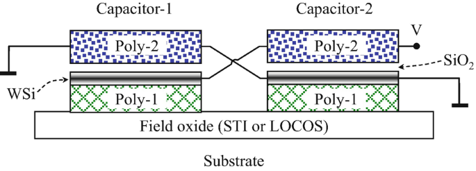
The figure below is a schematic of a precision analog capacitor with SiO2 as the dielectric, designed in a cross-coupled arrangement. Show that this arrangement reduces the VCC when compared to a single equivalent capacitor having the same dielectric.
-
6.
An MIM capacitor is formed with a triple ONO dielectric, consisting of 5-nm oxide, 10-nm nitride, and 10-nm oxide. Assume the dielectric constants to be 3.8 for oxide and 7.0 for nitride and
-
(a)
Find the equivalent oxide thickness teq and capacitance in fF/μm2.
-
(b)
For 5 V applied between the metal plates, calculate the fields in the oxide and nitride films.
-
(c)
For a maximum allowable field in the oxide of 5 × 10⁵ V/cm, what is the maximum voltage that can be applied to the capacitor?
-
(d)
What would be the maximum voltage if the dielectric was pure oxide of same teq as for the ONO structure?
-
(a)
-
7.
An accumulation-mode varactor of the type shown in Fig. 8.39 is formed between N+-polysilicon and N-well. The equivalent oxide thickness is 25 nm and the N-well concentration uniform with ND = 1017 cm−3. The gate voltage with respect to N-well is pulsed from +1 to −1 V. Assume negligible generation of electron–hole pairs, and find the tuning ratio at 25 °C. Neglect parasitic capacitances.
-
8.
The minimum top metal width and space in a CMOS process are, respectively, W = 0.5 μm and S = 0.5 μm. Use the minimum dimensions to design a square-shaped inductor of L = 10 nH. Disregard proximity and skin effects.

Rights and permissions
Copyright information
© 2020 Springer Nature Switzerland AG
About this chapter

Cite this chapter
El-Kareh, B., Hutter, L.N. (2020). Passive Components. In: Silicon Analog Components. Springer, Cham. https://doi.org/10.1007/978-3-030-15085-3_8
Download citation
DOI: https://doi.org/10.1007/978-3-030-15085-3_8
Published:
Publisher Name: Springer, Cham
Print ISBN: 978-3-030-15084-6
Online ISBN: 978-3-030-15085-3
eBook Packages: EngineeringEngineering (R0)