
Abstract
Chapter 6 provides further details of the converter synthesis algorithm. Key concepts covered in this chapter include data-buffers and data-related properties, converter definition and control, and the converter generation algorithm. We provide a classification of the inputs and outputs of a converter. Then the converter is formalized and its control actions are described using an example. The details of this algorithm with an appropriate illustration appears in Appendix A. This chapter may be viewed as the “converter synthesis” chapter.
Keywords
These keywords were added by machine and not by the authors. This process is experimental and the keywords may be updated as the learning algorithm improves.
In Chap. 4, we discussed the characteristics of SoCs and their behavioral models in terms of Synchronous Kripke structures. We have also presented SoC boilerplates to capture temporal logic formulas to succinctly and precisely capture the desired behaviors of SoCs. In Chap. 5, we discussed the problem of protocol mismatches, where independently-developed IPs are unable to “correctly” communicate with each other to realize the desired system. We showed how clock mismatches can be resolved using oversampling, and presented a methodology to resolve control and data-width mismatches using an automatic protocol conversion algorithm. In this chapter, we present the details of the protocol conversion methodology, primary focusing on the technical intricacies of dealing with data-width mismatches and the communication between the IPs and the converter to be generated to resolve the IP protocol mismatches. We also provide an outline of how converter generation can be achieved via the module checking technique described in Chap. 3.
6.1 Illustrative Example
Consider a SoC containing a master and a slave connected via the AMBA system bus Fig. 6.1,Footnote 1 the objective is to connect a consumer master to a slave memory block. The SoC bus requires the master to first request bus accessFootnote 2 through its arbiter and once access is granted, it can attempt to read data from the slave. We consider that the master and slave have some control and data mismatches, which hinder in their integration into the AHB system.

Convertibility verification overview
An Abstract Model. In order to illustrate such mismatches, we consider the abstracted behaviors of the SoC as presented in Fig. 6.2. Assume that the data-bus size of the AMBA AHB is 32 bits and all IPs use the bus clock to execute. Recall that, in our representation scheme (Definition 4.1 in Sect. 4.1), a transition is enabled and triggered only when the input signals (represented by conjunction of propositions) are present or absent (represented by negation). The transitions when executed can result in a set of outputs (or no output as represented by “ ⋅”).

Representation of the on-chip protocols of the IPs in Fig. 6.1. (a) Arbiter. (b) Slave writer. (c) Consumer master
Figure 6.2a shows the protocol P A of a bus arbiter that can arbitrate bus access between two masters (even though the SoC currently contains only one master). In its initial state a 0, the arbiter awaits bus request signals REQ1 or REQ2 from the masters, and grants access to the first requester by issuing the corresponding grant signal GNT1 or GNT2 respectively. In case both request signals are present at the same time, it gives access to master 1 by default. Master 2 is given access only when REQ2 is present and REQ1 is absent. Once access has been granted, the arbiter waits for the completion of a transfer by awaiting the RDY1 or RDY2 signals (depending on the active master), and then moves back to its initial state.
The slave memory block’s writer protocol P W is shown in Fig. 6.2b. In its initial state w 0, the protocol awaits the signal SELR (signifying a read request by the current master), and moves to state w 1. From w 1, in the next tick of the bus clock, the protocol enters state w 2. This transition results in the slave writing a 32-bit data packet to the SoC data bus (represented by the label Wrt 32 of the state w 2). After data is written, the protocol resets back to w 0.
The protocol P C for the consumer master is shown in Fig. 6.2c. From its initial state c 0, it keeps requesting bus access by emitting the REQ2 signal. When the grant signal GNT2 is received, it moves to state c 1 where it emits the control signal SELR (requesting a read from the slave) and moves to state c 2. It then awaits the control signal MORE to move to state c 3 (labeled by DIn 16), where it reads a 16-bit data packet from the SoC’s data bus. If the signal MORE is still available, the protocol can read multiple times from the data bus by making a transition back to c 3. When MORE is de-asserted, the protocol resets back to c 0.Footnote 3
The Protocol Mismatches. The various parts of the AMBA AHB system shown in Fig. 6.2 have the following inconsistencies or mismatches that may result in improper communication between them:
-
1.
Data-width mismatches: The consumer master has a data-width (word size) of 16-bits which differs from the word size of 32-bits for both the AMBA AHB bus and the slave memory. This difference in word sizes may result in improper or lossy data transfers. For instance,
-
(a)
Overflows: During one write operation, the slave protocol places 32-bits data to be read by the master onto the data-bus of the AMBA AHB (of size 32-bits). However, it is possible that the slave protocol attempts to write more data before the previous data has been completely read by the master.
In this case, some data loss may occur due to the overflow as the data-bus can only contain 32-bits.
-
(b)
Underflows: Similarly, if the master attempts to read data before the slave protocol has placed any data onto the data bus, an underflow may happen.
-
(a)
-
2.
Control mismatches: The exchange of some control signals between the various IPs of the system may result in deadlocks, data errors and/or the violation of bus policies when an IP produces some signals that are not consumed any other IP or when an IP expects a signal that is not produced by any other IPs. For instance,
-
(a)
Lack of synchronization: It is possible that the consumer master is reading data from the data-bus whereas the arbiter has reset back to its initial state (to signal the end of the transaction). This is possible because the reset signal RDY2 might be issued by the slave and read by the arbiter while the master is still reading data.
-
(b)
Missing control signals: The control signal MORE, required by the consumer master to successfully read data is not provided by any other IPs in the system. Without this signal, the master would deadlock at state c 2.
-
(a)
-
3.
Clock mismatches: There can be clock mismatches; however as discussed in Chap. 5, one can deal with clock mismatches by using oversampling (Definition 5.2). Oversampling each on-chip protocol creates a fully synchronous system. Henceforth, in this chapter we only consider the control and the data mismatches.
Objective. The objective of correct SoC design is to resolve the protocol (data and control) mismatches and additionally ensure the satisfaction of desired functionalities. We will show that the above objective can be encoded as CTL properties over states of IPs and SoC, and applying model/module checking based technique to generate a converter (if necessary and possible) which when composed with the given IPs satisfies the CTL properties (thereby resolving protocol mismatches and ensuring the satisfaction of desired functionalities).
6.2 Modeling Data as Labels on States
The first step in addressing data-width mismatches is to appropriately represent the size of the data being exchanged by IPs in an SoC and the channel associated with this data exchange. A channel here represents the buffer that is used for storing and retrieving the data being exchanged. Consider, for example, the 32-bit AMBA ASB data bus of the SoC in Fig. 6.1. Recall that SKS is used to represent the behavioural model of IPs and the communication model is concerned with the capturing the fact that some data (signal) is being exchanged between the on-chip protocols, rather than the contents of the data. Therefore, data operations can be captured by the data labels of the states in the SKS. Each data label must provide the following information:
-
1.
Data source: The data label must indicate the data channel to (from) which the data is written (read). Examples of data channels include the data bus and shared memories.
-
2.
Read or write: Each label must represent whether the data is being consumed or produced.
-
3.
Size of data: Each label must indicate the amount of data, in bits, being transferred.
The above information corresponding to the data labels can be captured as a mapping of each data label to a source, type, and size. For the SoC shown in Fig. 6.2, the data label Wrt 32 of the slave writer state w 2 is mapped to a write operation of 32 bits on the data bus. Similarly, the label DIn 16 of the consumer master state c 3 is mapped to a read operation of 16 bits from the data bus of the SoC.
In a more generic setting, SoC can contain multiple data channels and multiple read and write operations (captured by data labels in the SKS) for each data channel. For each data channel, we can assume that there are n data labels corresponding to read operations and m data labels corresponding to write operations in the SKS. For example, for the on-chip protocols presented in Fig. 6.2, the consumer master and the slave writer communicate over a common medium—the SoC data bus. The data labels DIn 16 and Wrt 32 in the SoC correspond to read and write operations from/to the data bus. Hence, in this case, n = 1 and m = 1, as shown in Fig. 6.3a. Figure 6.3b illustrates the more general case with m write and n read operations for a data channel. Each data operation (read or write) has its own size, or the number of bits transferred.

Data operations for a data channel. (a) Data operations for the case study. (b) Data operations in general
6.2.1 Data Constraints
Given the data labels, there are two types of constraints that are imposed for correct behavior. The first type can be viewed as “static” constraint, which is based on purely the size of the data being exchanged between communicating IPs. In other words, static data constraint does not rely on the dynamic behavior of the IPs. This constraint imposes a lower bound on the size of the data channel. The other type of data constraint is dynamic and is based on the behaviour of IPs. This constraint is specified using temporal logic and can be imposed on the communication behavior by appropriately constructing converters (as mentioned before). In the following, we will describe both these types of constraints.
Lower Bound on Medium Size. The lower bound on the size of the data channel via which data is being exchanged naturally depends on the size of the data being written to it and consumed from it. It is immediate that the lower bound is equal to the maximum size of the data that can be written to or read from a channel. That is, if k is the size of the data channel, then
where Wrt i (respectively, Rd i) is the data label corresponding to the i-th type of write (respectively, read) operation and Size( ⋅) represent the size of the data read and write. For instance, going back to Fig. 6.2, Size(DIn 16) = 16 and Size(Wrt 32) = 32, i.e., the size of the SoC data bus, k ≥ 32.
In addition to the above lower bound, it is also necessary to impose another condition on the data channel size. This condition requires that
-
1.
If the channel cannot accept any write operation, then it must have enough data to allow a read operation (shown as case 1 in Fig. 6.4).
-
2.
Similarly, if the channel contains data that is smaller than what any IP can read, then the channel must have enough space to allow a write operation (shown as case 2 in Fig. 6.4).

Computation of buffer bounds: Eq. 6.2.2
The above conditions can be expressed as a lower bound on the size of the medium k. We require that k must be large enough to allow the minimum sized read in the system when it does not have enough data for even the minimum sized write, and vice versa. The bound on k can be stated as follows.
where GCD is the greatest common divisor of the read and write data sizes. The minimum value of read/write operations and the GCD are used to capture the tightest lower bound for k. The minimum value provides the information regarding the smallest size for the read operation and the write operation. The GCD is subtracted to capture the fact that we are interested in the smallest number of read (or write) operations necessary to allow for at least one write (or read, respectively).
For our running example, \(k \geq [32 + 16] - 16\), i.e., k ≥ 32. While in this example, the necessary lower bounds as per the above two requirements are identical, there are cases where they may be different. Consider an example where
Then as per Eq. 6.2.1, k ≥ 10, and as per Eq. 6.2.2, k ≥ 12, which requires that k must be greater than equal to 12. Consider that 10 bits of data is written to the channel, the maximum number of reads (of size 4 bits) that are possible is 2 which results in 2 bits of data still present in the channel. At this point, no read operation is possible, however it is necessary to allow a write operation and that is why, the minimum size of the channel is set to 12.
Note that the lower bounds discussed above do not ensure deadlocks due to data-width mismatches between the IP-protocols can be avoided. This is because the protocols are not taken into consideration for identifying these bounds. Our objective, in this section, is to show the subtleties of the impact of data-width irrespective of the behavior exhibited by the IPs following different protocols. If the size of the channel is less than the lower bound, then there is a possibility of a deadlock. On the other hand, if the size of all the writes are the same and the size of all the reads are the same, then one can ensure that there will be no deadlock as long as the channel size is greater than the lower bound.
Dynamic or Temporal Data Constraints. So far, we have discussed the minimum size of the data channel which is likely to help avoid deadlocks in the communication between IPs. Dynamic data constraints, on the other hand, ensure the correct communication between IPs in terms of data-width. These constraints are impose temporal restrictions on the behavior of the IPs in terms of the data being written to and read from the data channel. Knowing the capacity k of the channel and ensuring that it satisfies the lower bound constraint as mentioned above, one can also keep track of the amount of data (yet to be consumed) present in the channel. A data counter, say cntr, can be maintained to capture the amount of data being written to and read from the channel. Whenever an IP moves to a configuration/state with a data label Wrt i, the counter is incremented by Size(Wrt i); on the other hand, whenever an IP moves to a configuration/state with a data lable Rd j, the counter is decremented by Size(Rd j). Finally, the temporal property
if satisfied by the behavior of the IPs, ensures that there is never any data overflow or underflow. Note that, in general such a property may not be satisfied by the IPs (due to protocol mismatch) and as a result, it is the job of a coverter to restrict the communication between the IPs in such a way that the above property is satisfied.
6.2.2 Control Constraints
As noted before, protocol mismatch due to lack of synchronization and missing signals are referred to as the control mismatch. Avoiding such mismatch will require that the IPs’ communication exhibit certain desired properties over control or are forced to exhibit the same due to the presence of a converter (responsible for mitigating protocol mismatches). We represent such properties in the logic of CTL.
Consider the illustrative example discussed in this chapter. One can require that the consumer master can always eventually read data from the system data bus. Such a property can be easily expressed using boiler plates described in the previous chapter. The CTL formula representing such a property will be
A similar property from the writer’s perspective is that the writer can always eventually write data.
An interesting property showing the interplay between control and data is when we require a control state to be reachable upon the satisfaction of certain data constraints, or vice versa. For instance, one may require that when all IPs are at their idle state, the data counter cntr must be equal to 0, or that the corresponding data channel must be empty.
6.3 Converters: Description and Control
Given the data and control constraints in terms of CTL properties, the objective is to ensure that communicating on-chip protocols and the data channels conform to those constraints, thereby, ensuring the absence of protocol mismatches. In the event, the communicating protocols do not satisfy the constraints, a converter (an intermediary) is installed between the on-chip protocols to regulate the communication between the on-chip protocols such that the data and control constraints are satisfied. Without loss of generality, we will consider that there are two protocols, P 1 and P 2, and a converter \(\mathcal{C}\), for the notational convenience. The parallel composition of P 1 and P 2 represented by the synchronous composition (see Definition 4.2) of SKSs (see Definition 4.1).
In order to regulate the communication between protocols, the converter acts as an intermediary which can relay and buffer signals between on-chip protocols as necessary. If all signals are exchanged between the protocols, then their parallel composition is closed. However, often the environment can play a vital role by providing inputs to on-chip protocols; such systems are called open systems. The function of the converter is to relay signals between protocols, between environment and protocols (when the system is open), and generate new signals for the protocols if necessary. The relay of signals between protocols can be delayed (by buffering) and therefore, can change the behavior of the system. In the following, we will describe the relationship of the input/output protocol signals of the protocols, environment and converter and then discuss the different types of signals based on what a converter can do with them (relay, buffer, hide, and generate).
6.3.1 I/O Relationship Between Converter, Environment and On-Chip Protocols
Consider the Fig. 6.5 to better understand the input/output relations between the converter, environment and on-chip protocols. Output from the environment and on-chip protocols are inputs to converter, \(I_{\mathcal{C}} = O_{env}\ \cup \ O_{1\vert \vert 2}\); while input to environment and on-chip protocols are produced as output from the converter \(O_{\mathcal{C}} = I_{1\vert \vert 2}\ \cup \ I_{env}\). Of course, some of the outputs from the on-chip protocols are consumed by the environment, while some of the outputs from the environment are consumed by the on-chip protocols: \(I_{env} \subseteq O_{1\vert \vert 2},O_{env} \subseteq I_{1\vert \vert 2}\). This indicates that the SoC is an open system which uses a subset of its inputs and outputs to interact with its environment (concepts of open and closed systems appear in Chap. 3).

The I/O connections between environment, converter and protocols
Going back to our illustrative example in Fig. 6.2, consider that a converter is placed as an intermediary between the on-chip protocols (arbiter, master and the slave) and the environment (responsible for producing necessary signals, e.g., REQ1). The converter reads all the signals generated by the environment and the participating protocols.
where signals REQ1 and RDY1 are generated in the environment (O env = {REQ1, RDY1}) and all other signals are emitted by the protocols. Similarly, the converter emits all signals meant for the environment and the participating protocols.
where the signal GNT1 is emitted by the converter to the environment (I env = GNT1) and all other outputs are meant for the protocols. It can be seen that the signal GNT1 emitted by the converter to the environment is read by the converter from the on-chip protocols and that the signals REQ1 and RDY1 read by the converter from the environment are emitted as converter outputs to the protocols (Fig. 6.6).

The I/O connections between on-chip protocols and the converter
6.3.2 Capabilities of the Converter
As mentioned in the previous sections, a converter can guide participating protocols by using the converter-environment-protocols I/O relationship. However, it should be noted that the converter has limited capabilities.
-
1.
Relay of signals: Converter can simply act as a relay and transfers signals between environment and on-chip protocols. For example, in Fig. 6.2 the converter must relay the input signal RDY1 generated by the environment to the arbiter.
-
2.
Disabling of signals: A converter may read an output signal from one on-chip protocol but hide it from another. This feature may help disable certain undesirable behaviour in the latter protocol. For example, in Fig. 6.2, a converter may disable the signal SELR, emitted by the consumer master from reaching the slave writer if there is not sufficient data contained in the shared memory.
-
3.
Buffering and event forwarding: A converter may read and buffer a signal from one on-chip protocol and then forward it to another protocol at a later stage. This may be needed to synchronize the protocols that do not necessarily move in a lock-step fashion, i.e., when one of them is emits a signal, the other is not ready to consume. For example, a converter may buffer the signal REQ2 emitted by the consumer master and forward it to the arbiter at a later stage.
-
4.
Generation of missing control signals: A converter may artificially generate signals that are not emitted as outputs by any participating protocols or the environment, but are required by the protocols as inputs. For example, a converter may generate the missing control signal MORE to ensure progress in the consumer master protocol shown in Fig. 6.2.
6.3.3 Types of Input/Output Signals of Converter
The capabilities of the converter is restricted to specific types of signals. For instance, a converter cannot delay and disable environment signals; it cannot artificially generate any signals that are produced by the environment or the protocols. As delaying and disabling can be viewed in similar light–disabling can be viewed as infinite time delay; we will consider broadly three types of input/outputs in a converter:
-
Uncontrollable [RW89]: These signals cannot be delayed or disabled by the converter.
-
Bufferred: These signals can be delayed or disabled by the converter.
-
Generated: These signals are generated by the converter as neither the protocols nor the environment produce these.
The uncontrollable events are further partitioned into signals emitted by the environment and protocols. In short, the types closely follow the sources of the signals. Table 6.1 succinctly represents the types. The first row shows the source and destination of signals; the second row shows whether the signal can be controlled or generated. The last two rows shows the notations we use to represent the corresponding input and output signals in the converter \(\mathcal{C}\). Figure 6.7 shows the I/O connections between converter, participating protocols and the environment. Buffered I/O is carried out when output signals emitted by the protocols are read in the converter’s buffers and emitted at a later stage. Generated I/O happens when the converter artificially emits input signals for the protocols. Finally, all uncontrollable inputs are read by the converter from the environment and are provided to the protocols immediately without buffering, and vice versa.

The different types of inputs and outputs of the converter
6.3.4 Description of Converter
Notations. Given a boolean formula b as a conjunction of literals i’s and their negations, we say that i ∈ b if and only if i is one of the literal appearing in a conjunct in b.
Given the types of converter inputs and outputs signals, we now define a converter as a finite state machine. Each state in the converter represents a configuration of the converter in terms of its control state and the set of the buffered signals. Each transition between converter states represents an evolution of the converter from one configuration to another. This converter SKS is described in Definition 6.1.
Definition 6.1 (CSKS).
A converter SKS \(\mathcal{C}\) is a \(\langle S_{\mathcal{C}},\) \(s_{\mathcal{C}0},\) \(I_{\mathcal{C}},\) \(O_{\mathcal{C}},\) \(R_{\mathcal{C}},\) clk⟩ where:
-
1.
\(S_{\mathcal{C}}\) is a finite set of states with \(s_{\mathcal{C}0}\) being the initial state.
-
2.
\(I_{\mathcal{C}}\) is the set of inputs partitioned into the following sets:
-
a.
The set \(I_{\mathcal{C}}^{unc}\) of uncontrollable environment inputs,
-
b.
The set \(I_{\mathcal{C}}^{buf}\) of buffered inputs, and
-
c.
The set \(I_{\mathcal{C}}^{emit}\) of uncontrollable protocol inputs.
-
a.
-
3.
\(O_{\mathcal{C}}\) is the set of outputs partitioned into the following sets:
-
a.
The set \(O_{\mathcal{C}}^{unc} = I_{\mathcal{C}}^{unc}\) of outputs to the protocols,
-
b.
The set \(O_{\mathcal{C}}^{buf} \subseteq I_{\mathcal{C}}^{buf}\) of buffered events to the protocols,
-
c.
The set \(O_{\mathcal{C}}^{emit} = I_{\mathcal{C}}^{emit}\) of outputs to the environment, and
-
d.
The set \(O_{\mathcal{C}}^{gen}\) of generated outputs
-
a.
-
4.
\(R_{\mathcal{C}}\subseteq [S_{\mathcal{C}}\times I_{\mathcal{C}}^{buf}] \times B(I_{\mathcal{C}}) \times {2}^{O_{\mathcal{C}}}\times [S_{\mathcal{C}}\times I_{\mathcal{C}}^{buf}]\) is a total transition relation. For any transition \((\mathrm{c},b){ I/0 \atop \longrightarrow } (\mathrm{c}^{\prime},b^{\prime})\), the following conditions hold:
-
a.
Immediate emission of uncontrollable signals:
-
i.
\(\forall i \in I_{\mathcal{C}}^{unc}: (i \in I\ \Leftrightarrow i \in O)\)
-
ii.
\(\forall i \in I_{\mathcal{C}}^{emit}: (i \in I\ \Leftrightarrow i \in O)\)
-
i.
-
b.
Correct buffering:
-
i.
\(O_{\mathcal{C}}^{buf}\ \cap \ O \subseteq b\)
-
ii.
\(b^{\prime} = (b/[O_{\mathcal{C}}^{buf} \cap O])\ \cup \ [O_{\mathcal{C}}^{buf} \cap \{ o\ \vert \ o \in I\}]\)
-
i.
-
a.
-
5.
All transitions in \(R_{\mathcal{C}}\) are synchronized with the ticks of the clock clk.
The above definition captures the converter behavior as follows. The converter inputs are all possible signals from the environment and the protocols. The converter emits the uncontrollable signals that are exchanged between the environment and the protocols immediately (as soon as it consumes such signals). The converter produces outputs for a protocol from its buffer if such outputs can be generated by some other protocol. Figure 6.8 illustrates a sample converter for the SoC shown in Fig. 6.2. Using this as an illustrative example, we explain the above definition:
-
States and initial state (point 1): The converter in Fig. 6.8 has a finite set of states {C0, …, C10} with C0 being the initial state.
-
Input and output classifications (points 2 and 3): As discussed in Table 6.1, the converter is able to read uncontrollable signals from both the environment and the protocols, as well as buffered inputs from the protocols. For the converter shown in Fig. 6.8, REQ1 and RDY1 are uncontrollable environment inputs, GNT1 is an uncontrollable protocol input, and REQ2, RDY2 and SELR are buffered inputs from the protocols. Similarly, the converter emits uncontrollable signals to the environment, and uncontrollable, buffered and generated signals to the protocols. For the converter shown in Fig. 6.8, REQ1 and RDY1 are uncontrollable outputs to protocols, GNT1 is an uncontrollable output to the environment, REQ2, RDY2 and SELR are buffered outputs to the protocols, and MORE is a generated output to the protocols.
-
Immediate relay of uncontrollable signals (point 4a): The converter immediately relays any signal that is to be exchanged between the on-chip protocols and the environment. For example, in the transition from state c2 to c1, the converter reads the uncontrollable signals REQ1 and GNT1, emitted by the environment and the arbiter protocol respectively. The converter immediately emits these signals as outputs of the same transition.
-
Correct buffering (point 4b): The converter maintains a one-place buffer for all signals that are exchanged between the protocols. This allows representing the buffered signals at any state Cg in the converter as a set b. Converter transitions are of the form \((\mathrm{C},b){ I/0 \atop \longrightarrow } (\mathrm{C}^{\prime},b^{\prime})\), where b is the set of buffered signals at state C and b′ is the set of buffered signals at state C′. In Fig. 6.8, the state of the buffer at a converter state is shown as the label of the state. For example, in state C0, the buffer is empty, and at state C1, the buffer is {REQ2}. Point 4b of Definition 6.1 constrains every transition of the form \((\mathrm{C},b){ I/0 \atop \longrightarrow } (\mathrm{C}^{\prime},b^{\prime})\) in the converter as follows. Firstly, we require a buffered signal to be present in the buffer b for it to be emitted during the transition from (C, b) (point 4b.i). For example, the transition from state C5 to C6 in Fig. 6.8 involves the emission of the buffered signal SELR. This transition is allowed only because the buffer at state C5 contains SELR. Secondly, point 4b.ii requires that when a transition is taken from state (C, b) to state (C′, b′), the buffer b′ at state C′ must contain any retained buffered signals from b (those that were not emitted during the transition) and all buffered signals read from the protocols during the transition. For example, in Fig. 6.8, the buffer is updated from ∅ to {SELR} to include the buffered signal SELR read during the transition from state C4 to C5.
Fig. 6.8 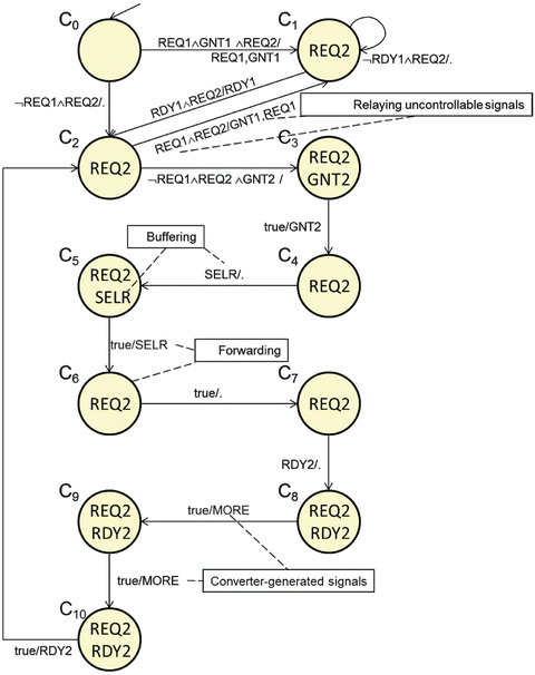
A converter for the SoC example presented in Fig. 6.2
Using sets to contain buffered signals means that a converter can remember only a single instance of a signal. In other words, we use converters with one-place buffers for control signals. One-place buffers guarantee that the converter buffer size is at most equal to the total number of signals that can be exchanged by the protocols, which in turn, ensures that the converter SKS model size is finitely bounded.
-
The converter can generate missing control signals that are needed by the on-chip protocols during any transition without restriction. For example, in Fig. 6.8, the converter generates the missing MORE during the two transitions from state C8 to C9 and C9 to C10.

6.3.5 Lock-Step Composition of Converter and On-Chip Protocols
A converter acts as an intermediary between protocols, and between protocols and the environment. It relays environment signals that it cannot enable or disable, suppresses/buffers some signals and generates signals as appropriate. The interaction between the converter and the protocols result in a new SKS model, whose inputs are the signals that are produced by the environment (for the protocols) and the outputs are the signals that are consumed by the environment (produced by the protocols). The interaction is described as a lock-step composition, the name suggests that for every moves in the protocols behavior, there exists a move in the converter. Figure 6.9 shows the lock-step composition of the converter \(\mathcal{C}\) shown in Fig. 6.8 and the synchronous composition (Definition 4.2) of the on-chip protocols shown in Fig. 6.2. As Fig. 6.9 illustrates, the lock-step composition of a converter and protocol (which can be a composition of protocols) is a SKS.

Each state in the lock-step composition corresponds to a state C in the converter and a state s in the synchronous composition. For example, the initial state of the lock-step composition SKS shown in Fig. 6.9 corresponds to the initial states C0 of the converter and \((a_{0},c_{0},w_{0})\) of the synchronous composition of the three on-chip protocols. The labels of every state (C, s) in the lock-step composition are the same as the labels of the constituent protocol state s. For example, state \(\mathrm{C}_{1},(a_{1},c_{0},w_{0})\) has the same labels Opt 1, Idle c and Idle w as state \((a_{1},c_{0},w_{0})\). Finally, each transition \((\mathrm{C},s)\stackrel{b/O}{\longrightarrow }(\mathrm{C}^{\prime},s^{\prime})\) between any two states (C, s) and (C′, s′) in the lock-step composition is described in terms of the transitions between states C and C′ in the converter and s and s′ in the protocols. Specifically,
-
1.
A transition from (C, s) to (C′, s′) exists if and only if state C has a transition to C′ and state s has a transition to s′. For example, in Fig. 6.9, state \(\mathrm{C}_{0},(a_{0},c_{0},w_{0})\) has a transition to state \(\mathrm{C}_{1},(a_{1},c_{0},w_{0})\) because states C0 and \((a_{0},c_{0},w_{0})\) have the following transitions to states C1 and \((a_{1},c_{0},w_{0})\):
 (6.3.1)
Henceforth, due to one-to-one correspondence between converter states and control buffers, we omit the reference to the buffers along converter transitions, and note only the converter states. For example, (C0, ∅) is noted as just C0.
-
2.
The transition from (C, s) to (C′, s′) contains an input signal i if:
-
(a)
i is an uncontrollable signal read by the transition from s to s′.
-
(b)
i is read as an input as well as emitted as an output signal in the converter transition from C to C′.
The two items above ensure that the converter relays uncontrollable signals immediately from the environment to the protocols. In the absence of any uncontrollable signal, the input label of the transition from s to s′ becomes true (Recall that input labels are boolean functions). For example, the input label of the lock-step transition from \(\mathrm{C}_{0},(a_{0},c_{0},w_{0})\) to \(\mathrm{C}_{1},(a_{1},c_{0},w_{0})\) contains the input signal REQ1 which is read as an input in the protocol transition and relayed by the converter transition (see Eq. 6.3.1).
-
(a)
-
3.
The transition from (C, s) to (C′, s′) contains an output signal o if
-
(a)
o is an uncontrollable signal emitted in the transition from s to s′, and
-
(b)
o is read as an input as well as emitted as an output signal in the converter transition from C to C′.
The two items above ensure that the lock-step composition immediately relays all uncontrollable signals emitted by the protocols to the environment. For example, the lock-step transition from \(\mathrm{C}_{0},(a_{0},c_{0},w_{0})\) to \(\mathrm{C}_{1},(a_{1},c_{0},w_{0})\) contains the uncontrollable output signal GNT1 which is emitted by the protocol transition and relayed by the converter transition (see Eq. 6.3.1 above).
-
(a)
-
4.
The transition from (C, s) to (C′, s′) does not contain an input signal i if i is a bufferable signal emitted by the transition from s to s′ and read by the converter in the transition from C to C′. For example, the transition from state \(\mathrm{C}_{0},(a_{0},c_{0},w_{0})\) to \(\mathrm{C}_{1},(a_{1},c_{0},w_{0})\) in Fig. 6.9 does not contain the bufferable signal REQ2 because it is buffered by the converter.
-
5.
The transition from (C, s) to (C′, s′) does not contain an output signal o if
-
o is a buffered signal emitted during the transition from C to C′, and read as an input in the transition from s to s′. For example, in Fig. 6.9, the transition from state \(\mathrm{C}_{5},(a_{2},c_{2},w_{0})\) to \(\mathrm{C}_{6},(a_{2},c_{3},w_{0})\) does not contain the (buffered) signal SELR emitted by the converter in the transition from C5 to C6 (Fig. 6.8).
-
o is a generated signal emitted by the converter during the transition from C to C′, and read as an input in the transition from s to s′. For example, in Fig. 6.9, the transition from state \(\mathrm{C}_{8},(a_{2},c_{2},w_{0})\) to \(\mathrm{C}_{9},(a_{2},c_{3},w_{0})\) does not contain the (generated) signal MORE emitted by the converter in the transition from C8 to C9 (Fig. 6.8).
-

The lock-step composition of the protocols in Fig. 6.2 and the converter shown in Fig. 6.8, as shown in Fig. 6.9, executes as follows. From its initial state \((\mathrm{C}_{0},(a_{0},c_{0},w_{0}))\), the converter lets the arbiter respond to the uncontrollable signal REQ1 to move to \((\mathrm{C}_{1},(a_{1},c_{0},w_{0}))\). In this transition, the converter makes REQ1 available to the protocols, and then emits the external output GNT1 (read from the arbiter) to the environment and buffers the signal RDY2 (read from the consumer master). In \((\mathrm{C}_{1},(a_{1},c_{0},w_{0}))\), the system waits for the uncontrollable signal RDY1 to reset to state \((\mathrm{C}_{2},(a_{0},c_{0},w_{0}))\). If however in state \((\mathrm{C}_{0},(a_{0},c_{0},w_{0}))\), the uncontrollable signal REQ1 is not read, a transition to \((\mathrm{C}_{1},(a_{0},c_{0},w_{0}))\) is triggered by the converter. During this transition, the converter reads and buffers the signal RDY2 (generated by the consumer master).
From \((\mathrm{C}_{2},(a_{0},c_{0},w_{0}))\), in the next clock tick, if the uncontrollable signal REQ1 is available, the system moves to state \((\mathrm{C}_{2},(a_{1},c_{0},w_{0}))\). Otherwise, a transition to state \((\mathrm{C}_{3},(a_{2},c_{0},w_{0}))\) is triggered. During this transition, the converter emits the previously buffered signal REQ2 (to be read by the arbiter). It then reads the signals GNT2,REQ2 from the protocols (emitted by the arbiter and the consumer master respectively) and buffers them. From \((\mathrm{C}_{3},(a_{2},c_{0},w_{0}))\) the converter passes the previously buffered GNT2 to enable a transition to \((\mathrm{C}_{4},(a_{2},c_{1},w_{0}))\). In the next tick, the converter reads and buffers the signal SELR (emitted by the consumer master) by triggering a transition to state \((\mathrm{C}_{5},(a_{2},c_{2},w_{0}))\). Then, the converter passes the buffered SELR signal (to be read by the writer slave) and the system makes a transition to state \((\mathrm{C}_{6},(a_{2},c_{2},w_{1}))\).
The converter then allows the protocols to evolve without providing any inputs. During this transition, the system moves to state \((\mathrm{C}_{7},(a_{2},c_{2},w_{2}))\). Note that \((\mathrm{C}_{7},(a_{2},c_{2},w_{2}))\) is a data-state because it is labelled by Wrt 32. This means that when the system reaches \((\mathrm{C}_{7},(a_{2},c_{2},w_{2}))\), the data-bus of the system contains 32-bits resulting in the data counter cntr being incremented to 32 (see Sect. 6.2.1 for details).
From \((\mathrm{C}_{7},(a_{2},c_{2},w_{2}))\), the system moves to \((\mathrm{C}_{8},(a_{2},c_{2},w_{0}))\) and the converter reads and buffers the input RDY2 (emitted by the writer slave). From \((\!\mathrm{C}_{8},(\!a_{2},c_{2},w_{0}))\!\), the converter generates the signal MORE, to allow a transition to \((\mathrm{C}_{9},(a_{2},c_{3},w_{0}))\). The converter then again generates MORE to move the system to state \((\mathrm{C}_{10},(a_{2},c_{3},w_{0}))\). Note that states \((\mathrm{C}_{9},(a_{2},c_{3},w_{0}))\) and \((\mathrm{C}_{10},(a_{2},c_{3},w_{0}))\) are data states as they are both labelled by DIn 16, which represents a 16-bit read operation. Hence, the counter is adjusted (decremented) to have values 16 and 0 respectively. Finally, from \((\mathrm{C}_{10},(a_{2},c_{3},w_{0}))\), the converter passes the previously buffered signal RDY2 (to the arbiter) allowing the system to move to state \((\mathrm{C}_{2},(a_{0},c_{2},w_{0}))\).
6.4 Generating Converters Using Module Checking
We have discussed three important aspects in SoC design so far. We have described how the protocols are composed, which represents all possible behavior of the participating protocols (see Definition 4.2 in Sect. 4.1.2). We use temporal logic to formally represent the desired behavior of the protocols with respect to the control signals and data-width (see Sects. 4.2 and 6.2). We have also described how a converter interacts with the protocols and can potentially regulate the behavior in the interaction (see Sect. 6.3).
The final piece in our setup is the method that can be used to generate converters (if possible) automatically such that the generated converter interacts with the protocols and satisfy the desired behavior as specified using temporal logic. The method directly follows from the module checking algorithm discussed in Sect. 3.2. Under special cases, when there are no uncontrollable signals and the composition of on-chip protocols is closed, model checking may be used [SRB08a].
Recall that, the central theme for module checking as described in Sect. 3.2 is that
-
1.
A module does not satisfy a property if and only if there exists some restricted behavior in the module which does not satisfy the property (or satisfies the negation of the property) under consideration, and
-
2.
Existence of such a restricted behavior can be verified by generating a “environment” which forces such a restriction.
In Sect. 3.2, we have discussed how such an environment can be automatically generated using a tableau-based algorithm. The same idea can be applied in SoC and protocol conversion. The objective is to restrict the behavior of the protocols in such a way that the restricted behavior satisfies certain desired property. The restriction is realized by generating a converter (if possible). Therefore, the correspondence is as follows:
-
The composition of protocols is the module in a module checking.
-
The lock-step composition of protocols and the converter (to be generated) corresponds to the parallel composition between the module and its “environment”.
-
The desired properties of the protocols to be enforced by the converter correspond to the negation of the properties satisfied by the module in some environment.
-
The environment identified as part of module checking corresponds to the converter in the context of protocol conversion.
Of course there are some important distinguishing factors—for instance, in module checking, we consider that a state emitting uncontrollable signals does not emit controllable ones (system state) and vice versa (environment state); on the other hand, in protocol conversion, the protocols can produce and consume both controllable and uncontrollable signals from the same state. The difference is due to the difference in the semantics of the parallel composition between module and its environment and the lock-step composition between the protocols and their converter. However, the basic principles of the converter in protocol conversion and the environment in module checking remain identical, i.e., control the controllable signals, relay/allow the uncontrollable ones.
The converter shown in Fig. 6.8 can be generated using our algorithm such that it can control the composition of the protocols shown in Fig. 6.2 such that all mismatches are resolved, and all system-level control and data constraints are satisfied. The resulting lock step composition is shown in Fig. 6.9. We have adapted the module checking approach and developed a converter synthesis approach that is presented in Appendix A.
6.5 Concluding Remarks
This chapter presented a unifying approach towards performing protocol conversion with control and data mismatches. Earlier works could only handle control or data mismatches separately or handle both in a restricted manner. The fully automated approach is based on CTL module checking, allowing temporal logic specifications for both control and data constraints. Converters are capable of handling different types of I/O signals such as uncontrollable signals, buffered signals and missing signals in the given protocols. Appendix A provides the details of the converter generation algorithm, with an example to illustrate its operation. The next chapter provides a detailed review of related work for SoC design and system-level verification of SoCs.
Notes
- 1.
A similar example with two masters and one slave was presented in Fig. 4.1 in the last chapter.
- 2.
For the time being, readers can ignore the presence of “Converter” between the Master and the SoC Bus.
- 3.
The use of MORE captures a typical burst transfer operation in SoCs where a master may allow multiple data transfers during the same bus transaction.
References
P.J.G. Ramadge, W.M. Wonham, The control of discrete event systems. Proc. IEEE 77, 81–98 (1989)
R. Sinha, P.S. Roop, S. Basu, A model checking approach to protocol conversion. Electron. Notes Theor. Comput. Sci. 203(4), 81–94 (2008)
Author information
Authors and Affiliations
Rights and permissions
Copyright information
© 2014 Springer Science+Business Media New York
About this chapter
Cite this chapter
Sinha, R., Roop, P., Basu, S. (2014). Automatic Protocol Conversion. In: Correct-by-Construction Approaches for SoC Design. Springer, New York, NY. https://doi.org/10.1007/978-1-4614-7864-5_6
Download citation
DOI: https://doi.org/10.1007/978-1-4614-7864-5_6
Published:
Publisher Name: Springer, New York, NY
Print ISBN: 978-1-4614-7863-8
Online ISBN: 978-1-4614-7864-5
eBook Packages: EngineeringEngineering (R0)