Abstract
As intended by its name, physically unclonable functions (PUFs) are considered as an ultimate solution to deal with insecure storage, hardware counterfeiting, and many other security problems. However, many different successful attacks have already revealed vulnerabilities of certain digital intrinsic PUFs. This paper demonstrates that legacy arbiter PUF and its popular extended versions (i.e., feed-forward and XOR-enhanced) can be completely and linearly characterized by means of photonic emission analysis. Our experimental setup is capable of measuring every PUF internal delay with a resolution of 6 ps. Due to this resolution, we indeed require only the theoretical minimum number of linear independent equations (i.e., physical measurements) to directly solve the underlying inhomogeneous linear system. Moreover, it is not required to know the actual PUF responses for our physical delay extraction. We present our practical results for an arbiter PUF implementation on a complex programmable logic device manufactured with a 180 nm process. Finally, we give an insight into photonic emission analysis of arbiter PUF on smaller chip architectures by performing experiments on a field programmable gate array manufactured with a 60 nm process.
1 Introduction
Physically unclonable functions (PUFs) [18, 34] are introduced to overcome the drawbacks of traditional key storage and key generation techniques. PUFs can be utilized as the basis for many security applications, such as encryption [23, 43] and hardware fingerprinting [39, 51]. Although there are different PUF classifications in the literature regarding their characteristics, intrinsic PUFs can generally be categorized into two distinct classes: settling-state-based PUFs and timing-based PUFs [24]. The former is based on bistable circuits such as SRAM cells, while the latter is based on intrinsic differences in timing of a set of symmetric circuit paths. While settling-state-based PUFs are utilized as key storage on a chip, timing-based PUFs are most preferred in cryptographic protocols [7, 8].
Previous work in the literature has shown how different PUFs can be attacked and cloned. Settling-state-based PUFs such as SRAM PUFs can be characterized and cloned by noninvasive and fully-invasive attacks [19, 31, 32]. However, timing-based PUFs in general are more complex to be physically cloned due to their interconnected structures. The main assumption of timing-based PUFs is that only fully-invasive techniques enable an attacker to measure the individual delays within the PUF structure. These kind of attacks might alter the physical properties of the silicon substrate, which leads to undesirable changes in the challenge-response-pair (CRP) behavior of the PUF. Hence, the existing attacks are limited to response emulation of the timing-based PUFs either by noninvasive modeling attacks [9, 14, 22, 36] or side-channel attacks [27–29, 38].
This work demonstrates that the main assumption on the infeasibility of direct delay measurements in timing-based PUFs is not valid. We will present how arbiter PUFs and more generally, timing-based PUFs can be characterized by a high-resolution temporal photonic emission analysis from the chip’s backside. This approach does require neither any readout of PUF response nor a substantial number of challenges to characterize the PUF. Our methodology is based on measuring the time difference between enabling the PUF and photon emission at the output of the last stage. For our proof of concept (PoC), we have implemented arbiter PUFs on the common programmable logic devices. The delay between the input of the PUF and the output of photodetector can be measured with an overall resolution of approximately 6 ps by a time-to-digital converter (TDC). As a result, the PUF response is determined by comparing the measured delays on both PUF chains. Furthermore, in our methodology, the number of challenges required for the physical characterization of the PUF increases linearly with the PUF length. Finally, based on a mathematical approach we find the minimum number of necessary challenge combinations, which are required to characterize the PUF.
1.1 Contributions
The main contributions of this paper are as follows:
Physical characterization of timing-based PUFs. We present a novel physical characterization attack on timing-based PUFs with the help of photonic emission analysis. This approach is capable of physically characterizing the intrinsic behavior of the circuit by measuring the delays within the circuit with a high degree of accuracy. In the case of an arbiter PUF, this consists of measuring the intrinsic delays of each individual stage of the circuit. As compared to other heuristic methodologies which require a substantially greater number of measurements than individual PUF stages, our methodology requires just two measurements per PUF stage.
Low-cost measurement setup for measuring the delay with the resolution of 6 ps. We introduce an efficient and cost-effective experimental setup with a substantial temporal resolution. The setup is capable of performing temporal measurements with an approximate time resolution of 6 ps. The time resolution of the setup allows for the exact characterization of the intrinsic delays of each individual stage of the PUF.
Practical evaluation against a proof-of-concept arbiter PUF implementation. The PoC implementation was realized on the common programmable logic platforms. To extract the device’s intrinsic behavior, we performed dynamic semi-invasive backside analysis of the photonic emissions of the device. Because the analysis techniques are semi-invasive, the integrity of the device’s intrinsic response is not changed.
Mathematical approach for measurement optimization. In order to physically characterize the PUF, we propose a measurement technique to minimize the number of challenges that are necessary for a PUF characterization. Furthermore, we provide a mathematical approach for minimizing the effort of measurement for arbiter PUFs in general. Combined, these techniques greatly reduce the number of measurements and measurement locations that are necessary for PUF characterization.
1.2 Organization
This paper is organized as follows: Sect. 2 presents background information on the delay-based PUFs and photonic emission in CMOS technology. Moreover, the programmable logic architecture is explained and the related work is reviewed. In Sect. 3, the utilized experimental setup is presented. Section 4 introduces the mathematical approach for the optimized measurement. Section 5 demonstrates the practical results, where we were able to measure the small delay differences and characterize the PUF. In Sect. 6, we present additional considerations about our methodology. Furthermore, we give an insight into physical characterization of arbiter PUFs implemented on smaller integrated circuit (IC) technologies. Finally, in Sect. 7, we conclude the paper.
2 Background
2.1 Arbiter-Based PUF
Due to manufacturing variations, there are small random delay differences on symmetrical electrical paths on a chip. The entropy of the delays is sufficient to ensure a unique PUF response for each individual device instance. Arbiter and RO PUFs are two examples of timing-based PUFs [25]. Arbiter PUF utilizes the intrinsic timing differences of two symmetrically designed paths to a single bit of the response at the output of the circuit [22]. It consists of multiple connected stages and an arbiter at the end of the chain, see Fig. 1. Each stage consists of two outputs and three inputs, a single bit of the challenge and the two outputs from the previous stage. The inputs of the first stage are connected to a common enable signal. The outputs of the last stage are connected to a so-called arbiter, which determines which signal arrived first. Based on this result, the arbiter generates a single bit known as the response. Although the nominal delays of direct paths and crossed paths are equal (\(\delta _{i_{a}}=\delta _{i_{d}}\) and \(\delta _{i_{b}}=\delta _{i_{c}}\)), due to the intrinsic delays of the circuit, different challenges produce different results. In an ideal arbiter PUF, the differences between two identical device instances will be sufficient to differentiate the unique responses of the devices. The main security assumption is that an attacker cannot measure individual delays of an arbiter PUF without destroying it (i.e., changing its CRP behavior). Therefore, in the best case the attacker can only intercept the applied challenges and generated responses.
2.2 Photonic Emission in CMOS
Individual logic gates are implemented on the complementary metal oxide semiconductor (CMOS) ICs by a set of connected p-type and n-type metal oxide semiconductor (MOS) transistors. In a static state, where no transistor devices are switching, there is at least one transistor in the off region between the supplied power (VDD) and ground (GND). Therefore, the current consumption of the gate is minimal. However, during a switching event a substantial current passes through the circuit. As a result, the transistors enter an operating region known as saturation for a short period of time. During saturation, the kinetic energy of accelerated hot carriers can be released via photon emission [5]. n-type transistors emit significantly more photons as compared to p-type transistors, due to the higher mobility of electrons than holes. The emission rate of the transistors is proportional to the switching frequency of the circuit. However, raising the supply voltage also increases the amount of photons emitted by the device exponentially.
Due to multiple interconnect layers on the frontside of modern IC designs, the optical path is obstructed [35]. Therefore, it is almost impossible to observe photonic emissions from the IC frontside. However, photonic emissions can be observed from the IC backside. Although silicon substrate is highly absorptive for wavelengths shorter than the bandgap energy, the silicon substrate is transparent to near-infrared (NIR) emissions. Hence, any NIR photons emitted by the device will pass through the silicon substrate and can be observed from the IC backside.
The CPLD LUT is realized by multiple multiplexers, which are controlled by the data inputs. The output of the LUT is loaded from the existing SRAM cells inside the LUT. By connecting don’t-care inputs A, B and C to a single bit challenge and connecting the input D to the output of previous stage, only two routes can be selected based on the challenge value
2.3 Programmable Logic Architecture
PUFs can be realized in different types of hardware implementations. Timing-based PUFs can be implemented on the common programmable logic devices, such as FPGAs and CPLDs. The architecture of modern CPLDs and FPGAs is very similar, and the architectures of any given vendor share many commonalities. The primary architectural differences of modern CPLDs and FPGAs are logical size, the complexity of the routing network and the hard macros available to the design. Moreover, CPLDs generally store the configuration within the same device package, whereas FPGAs generally require external memory for storing the device configuration. Programmable logic devices consist of an array of configurable logic elements (LEs). The configuration determines the logical behavior of each individual LE. The LEs themselves are commonly realized using so-called lookup tables (LUTs) in which the output values are stored for a particular input combination. Combinatorial logic of a particular design can be entirely realized using LUTs. The Altera Max V CPLD architecture utilized in this work has a 4-input LUT, see Fig. 2. Each LE also provides an additional configurable register with multiple control inputs and an output for realization of sequential logic. Multiple LEs in a group form so-called logical array blocks (LABs). In addition to global routing resources, each LAB provides additional routing to each LE within the LAB.
2.4 Related Work
2.4.1 Attacks on PUFs
In recent years, many different attacks on PUFs have been proposed. Settling-state-based PUFs, such as SRAM PUFs, can be physically cloned by a focused ion beam (FIB) circuit edit [19]. Moreover, it has been shown that SRAM PUFs are vulnerable to invasive attacks, due to lack of tamper detection mechanism [31]. Besides, memory-based PUFs can be cloned by a side-channel attack based on remanence decay in volatile memory [32]. Finally, the vulnerabilities of the memory-based PUFs in general as a replacement for nonvolatile memory are reviewed [20].
In contrast to settling-state-based PUFs, timing-based PUFs (e.g., arbiter PUFs and RO PUFs) are believed to be resistant to physical clone, due to their more complex structures. It was shown that RO PUFs are vulnerable to the electromagnetic (EM) side-channel attacks [27–29] and modeling attack [15]. However, arbiter PUFs have been frequently target of mathematical modeling attacks. Therefore, the known attacks in the literature try to emulate the CRP behavior of the PUF and build a mathematical clone of it. Modeling attacks require a subset of CRPs to build a model on that and predict the PUF response for all possible challenges [22]. One of the first utilized modeling techniques was linear programming to model the timing-based PUF [33]. Recently, it has been shown that how an arbiter PUF under the deterministic finite automata (DFA) representation can be probably approximately correct (PAC) learned with a given level of accuracy and confidence [14].
The modeling attacks become more difficult by introducing nonlinearities to the PUF delays and responses. Two examples of nonlinear PUFs are feed-forward arbiter PUFs [23] and XOR arbiter PUFs [47]. However, it has been shown that feed-forward PUFs are vulnerable to evolutionary algorithm [37]. Moreover, a successful modeling attack on XOR arbiter PUFs with a limited number of arbiter chains using logistic regression (LR) algorithm is reported [36]. In another attempt, by PAC learning the XOR arbiter PUF with the perceptron algorithm, a theoretical limit as a function of the number of PUF stages and the number of chains for pure modeling attack could be found [16]. Although pure modeling attacks fail to learn larger XOR arbiter PUFs, a combined modeling attack based on higher number of CRPs with timing and power side-channel information can successfully break XOR arbiter PUFs up to 14 arbiter chains [38]. Recently, a novel approach based on lattice basis reduction and photonic emission analysis is introduced, which can break a controlled XOR arbiter PUF with very large number of chains [13]. In another approach, the noise in the response of the arbiter PUF was exploited as a side-channel information to model the CRP behavior of the single arbiter PUF [9]. The idea of using noise as an helper information to improve modeling attacks is further developed by changing the temperature [10] and supply voltage of the chip [4] to induce more noise in the PUF responses. Furthermore, it has been shown that individual chain of an XOR arbiter PUF can be separately learned by using the noise information in the CMA-ES algorithm [3]. Finally, a combination of laser fault attack and machine learning is reported recently in the literature, which break the security of the XOR arbiter PUFs with arbitrary number of arbiter chains [49].
2.4.2 Photonic Emission Analysis
Photonic emission analysis is introduced as a new side-channel attack to analyze security applications on the chip such as cryptographic ciphers [12]. In order to bypass the multiple interconnect layers on the frontside of the chip, photonic emission analysis and photonic fault injection attacks can be conducted from the backside [11, 44, 45]. It has been shown that chips, such as microcontrollers, can be functionally analyzed by their optical emissions during runtime [30]. Simple Photonic Emission Analysis (SPEA) is another approach that can recover the full AES secret key by monitoring access to S-Box [42]. Furthermore, the full AES secret key can be recovered by a similar approach called Differential Photonic Emission Analysis [21]. Recently, it has been shown how different combinatorial and sequential logic primitives on the hardware implementations, such as programmable logic, can be located and identified by photonic emission analysis [50]. In another attempt, time-integrated and time-resolved emission measurements are utilized to identify and localize logical state changes and functional block activity inside a chip [46].
3 Experimental Setup
3.1 Measurement Setup
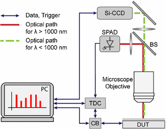
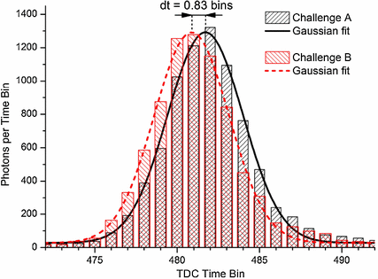
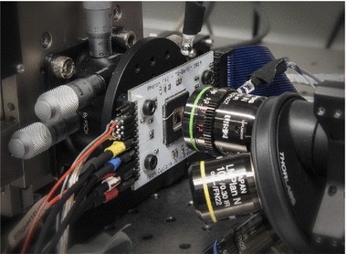
The experimental setup, as schematically shown in Fig. 3, is an optimized infrared microscope equipped with a scientific Si-CCD camera and an InGaAs avalanche diode as detectors for spatial and temporal analysis [41]. The Si-CCD is a back-illuminated deep depletion type featuring high quantum efficiency in the NIR region. To minimize dark current, it is cooled down to \(-70\,^{\circ }\hbox {C}\), which allows long exposure times to accumulate enough photons from the weak hot carrier emission. Due to the long integration time of several seconds and the limited readout speed of the CCD sensor, it is used for spatial analyses only. The temporal analysis of the photonic emission requires a very fast infrared detector. Therefore, a free-running InGaAs avalanche detector in Geiger mode (SPAD) is used to detect single photons. Its sensitivity covers a wavelength range between 1 and \(1.6\,\upmu \hbox {m}\) with peak quantum efficiency of 20 %. Thermoelectrical cooling reduces the dark count rate below 2 kHz. The device under test (DUT) is controlled by a computer via a control box (CB), which provides the enable signal for the PUF and a time reference signal for the time-to-digital converter (TDC). Photons emitted from the DUT are collected by the microscope objective (NA = 0.6) and divided into two optical paths by a short-pass beam splitter (BS). Short-wave photons below 1 \(\upmu \)m are transmitted to the Si-CCD camera, while the long-wave photons are reflected onto the InGaAs-SPAD. This configuration allows capturing images with the CCD and time-resolved measurements with the SPAD simultaneously. An incoming photon from the DUT causes the avalanche breakdown of the SPAD, and the resulting electrical pulse is registered by the TDC. The FPGA-based TDC time tags each occurring event with a resolution of 81 ps. This way both the enable signal of the PUF chain and the detected photons from the chain’s output transistor are time tagged allowing a direct calculation of their delay. Due to jitter in the response time of the SPAD and electrical jitter in the CB and TDC, the overall time uncertainty for a single photonic event is 190 ps rms. An accumulation of multiple photonic events is used to improve the time resolution by calculating the centroid of the Gaussian-like distribution of the delay time histogram, see Fig. 4. This super-resolution technique enhances the time resolution significantly beyond the 81 ps granularity of the TDC and allows measurements of very small shifts in the delay time. Experiments showed that the accuracy of our current setup is limited by drifts in the electronics to 6 ps rms. Apart from the custom-made holding of the DUT to a 3-dimensional moving stage and electronics to control and communicate with the CPLD, the setup consists of commercially available components. As the focus of the setup is on time-resolved measurements, it can be realized for about 30000 Euros.
3.2 Device Under Test
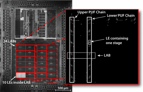
In this work, Altera devices MAX V CPLD (part number 5M80ZT100C5N) were utilized for the physical experiments [1]. A backside reflectance image of the CPLD shows the presence of 240 LEs on the device, see Fig. 5. However, this device allows the use of 80 Logic Elements (LE) in total. The device contains 24 logic array blocks (LAB) with 10 LEs each. The nonvolatile memory and additional infrastructure logic are located on the upper half in Fig. 5, and I/O pads are clearly visible on the perimeter of the device. The bulk silicon material of the devices was thinned down significantly. The silicon surface was polished to expose a surface suitable for optical imaging. Finally, the devices were soldered onto a custom printed circuit board (PCB) to allow capturing of images from the exposed backside of the device while maintaining full electrical connectivity.
The backside reflectance image acquired using a laser scan microscope (left). Inside the framed area, all programmable logic cells are located. The grid corresponds to the placement of 4 by 6 LABs with additional routing infrastructure in-between. Within each LAB, 10 LEs are located (only a single LAB is shown containing the LEs). Optical emission of the 8-bit arbiter PUF on the CPLD (right). Each stage is realized by two LEs in a LAB in parallel
3.3 PUF Implementation on Programmable Logics
One possibility for implementing arbiter PUFs is to utilize digital multiplexers. In this case, each PUF stage requires two multiplexers. As each multiplexer is realized by a LUT, two inputs out of four available inputs of a LUT are utilized, see Fig. 2. Based on don’t-care inputs, the output of multiplexer can be loaded from different SRAM cells inside the LUT and take different routes to the output. This fact leads to dependency of the PUF response not only on the delays of the individual routes within an LUT but also on the arrival time of the signal from the previous stage. Consequently, delay imbalances will occurred for two PUF chains and the linear additive model of the arbiter PUF is not valid anymore. Therefore, we have implemented each stage of the PUF by two independent LUTs as in [26], where only one input of each LUT is utilized as the stage input and all other don’t-care inputs are connected together to a single challenge bit, see Figs. 5 and 6. As a result, by applying a challenge bit only two different routes can be selected inside the LUT, see Fig. 2.
To validate our concept, the design consists of an 8-bit arbiter PUF on the CPLD. Each stage is placed manually in an individual LAB to make the PUF chains symmetric. Due to very little delay differences between two chains, the arbiter can sample a metastable signal. Moreover, due to asymmetric length of data and clock lines, the delay between the outputs of the last stage and the inputs of the arbiter cannot be designed symmetrically. Hence, instead of using an arbiter, we readout the response by measuring the overall delays of both chains with the help of photonic emission analysis.
4 Measurement Approach
For completeness, we present in this section two approaches to solve the underlying linear system of arbiter PUFs—first, the slightly more elaborate approach for MUX-based PUFs although it is unnecessary for our PoC implementation. Second, the related but simpler approach for our delay-based PUF implementation.
Binary vectors are denoted with the bold lowercase letters, e.g., \(\mathbf{r}\). Their elements are selected with an index \(i \ge 1\) in subscript, e.g., \(\mathbf{r_{1}}\), \(\mathbf{r_{2}}\), etc. Binary matrices are printed with the bold uppercase letter, e.g., \(\mathbf{C}\). Scalars are denoted with the italic lowercase letters, e.g., n.
4.1 Optimized Measurement for Ordinary MUX-based PUF Characterization
In a MUX-based arbiter PUF, each stage consists of four different propagation delays: two direct path delays and two switching path delays, see Fig. 1. In order to completely characterize an n-stage arbiter PUF, all propagation delays of each stage have to be known; hence, 4n delays must be characterized in total. One conceivable way would be to naively measure all 4 propagation delays at all n stages individually by moving the optical setup over both inputs and both outputs of each stage, and simply try both challenge states. However, this technique would require the movement of the chip and adjusting the focus for each movement. As our setup has a very high spatial resolution, a precise aperture movement can be automated and eventually yield the 4n arbiter delays. While practically certainly feasible and also theoretically optimal, we can do much better in terms of physical measurement efforts. A more intelligent solution will simply try to measure the overall propagation delays of each PUF chain at the outputs of the very last stage for sufficiently many selected challenge combinations. As the overall delay at the outputs of the last stage is the sum of all n delays in each stage, cf. additive linear model due to [23], every measurement has to consider for every chosen challenge the complete propagation time of two distinct but possible paths—the upper output (D input to sampling flip-flop) and the lower output (C input to sampling flip-flop). If we denote by \(r_i\) the resulting overall time of an individual challenge measurement, we conclude that we get an inhomogeneous system of linear equations
for our 4n unknowns \(\delta _{i_{a}}, \delta _{i_{b}}, \delta _{i_{c}},\) and \(\delta _{i_{d}}\) and the challenge matrix \(\mathbf{C}\) with entries from \(\{0, 1\}\) which encode the different valid paths through the arbiter chain. We call a path \(\mathbf{c}_i \in \{0,1\}^{4n}\) valid if its respective challenge setting within \(\mathbf C\) allows a full signal propagation of length n, i.e., until its very end. By induction the following is easy to see.
Proposition 1
For an arbiter PUF of length \(n \ge 1\) let \(\mathbf C\) be the \((2^{n+1}) \times (4 n)\) matrix consisting of all valid paths through the respective arbiter chain. Then, \(\mathrm{rk}(\mathbf{C}) = 2 n + 2\).
Seeing now that we have only \(2n + 2\) linear independent equations in \(\mathbf{C}\), we need to generate the remaining \(2 (n-1)\) linear independent equations to completely solve our system in another way. Thus, we are forced to consider also partial valid paths instead of full propagation paths. Let \(\mathbf{c}_i \in \{0,1\}^{4n}\) be a valid path; for integers \(1 \le u, v \le n\) a vector of the form
will be called a partial valid path.
Note 1
For a partial valid path, we will measure its signal time only from the inputs of arbiter stage u until its output at stage v and deliberately denote this partial time simply also by \(r_i\).
Including such partial measurements \(r_i\) (i.e., including measurements within the arbiter chain) and their corresponding paths \(\mathbf{c}_i\), we also get by induction.
Proposition 2
For an arbiter PUF of length \(n\ge 1\) and its \(2n + 2\) valid paths (corresponding to the linear independent row vectors), there exist \(2 (n-1)\) appropriate partial valid paths such that their combined challenge matrix \(\mathbf{C}\) has full rank 4n.
This Proposition implies that we only need \(2 (n-1)\) partial measurements which we classify with respect to u and v into three classes:
-
1.
\(u=1\) and \(1 \le v <n\): Measurement begins at the inputs of the first stage and ends in the middle of the chain.
-
2.
\(1 < u, v < n\): Measurement starts at some inputs in the middle of the chain and also ends in the middle of the chain.
-
3.
\(1< u \le n\) and \(v=n\): Measurement starts at the inputs in the middle of the arbiter chain and ends after the last stage.
In order to keep the previously discussed physical measurement efforts minimal, it is therefore obvious to generate the missing linear independent equations out of group 1 or 3—dependent on varying setup advantages. This completes our description of an optimized measurement for a classical MUX-based PUF with n stages.
4.2 Simplified Measurement for Delay-Based PUFs
As we already pointed out in Sect. 2.1, we have \(\delta _{i_{a}} = \delta _{i_{d}}\), and \(\delta _{i_{b}} = \delta _{i_{c}}\) for their respective inverters. Moreover, as the two paths, i.e., the upper and the lower path, are not crossing at all, in other words they are disjoint, we can consider them completely separately, see Fig. 6. Toward this, let us consider the upper path and simply denote its n unknown delays by \(\delta _1, \ldots , \delta _n\). I.e., setting the respective ith challenge bit to 1 adds the delay \(\delta _i\) to the overall complete signal propagation time which will be denoted by \(r_j\) for the jth measurement from the first input until the last output—just through all n stages. If we now define the distinguished variable \(\Delta _{n+1}\) as the overall complete signal propagation time for setting all n challenge bits to 0, we get the (already solved) linear system
for which we simply require the measurements \(r_{i}\), \(i=1, \ldots , n+1\). The lower path can be handled in an analog way, say \(\mathbf{C}' \cdot \varvec{\Delta }' = \mathbf{r}'\). Moreover, using the unit vectors \(\mathbf{e}_i \in \{0, 1\}^{n+1}\), \(i=1,\ldots , n+1\), we find that we get from
the two individual inverter delays \(\delta _i\) and \(\delta '_i\) of stage i incurred by setting the ith challenge bit to 1. We thus conclude that we need only \(2n+2\) “full path" measurements to completely characterize a delay-based PUF with n stages.
5 Results
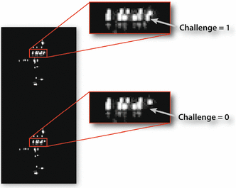
We have chosen the challenge 00000000 as the reference challenge for our measurements on the CPLD. In order to measure the effect of each challenge bit, we have applied the challenge combinations with hamming distance one to see the effect of each challenge bit individually. The enable signal was switched with a frequency of 4 MHz, and the chip was supplied with 2.2 V. The optical emission of the PUF circuit reveals the position of each stage, see Fig. 5. Moreover, the inputs and outputs of each stage for measurement can also be found on this emission image. If there is no electrical access to challenges, comparing the optical emission of the PUF stages can also reveal the state of individual challenge bits. By changing each challenge bit, the emission pattern of each LE is changed, and therefore, the challenge can be read without any electrical access to it, see Fig. 7. Therefore, the equations provided in Sect. 4 can still be used to characterize the PUF by finding challenges with hamming distance one from each other.
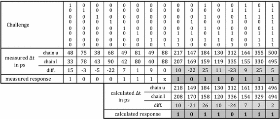
We repeated the measurement 50 million cycles to capture enough number of photons for analysis. The reference challenge also has been measured multiple times during our experiments to compare the consistency of measurements. The measurement results of 8 challenge combinations compared to the reference challenge can be found in Fig. 8. Positive timing difference means that the delay is decreased in comparison with the reference challenge and vice versa. It can be seen that flipping the challenge bit from 0 to 1 makes in all cases both upper and lower chains faster. Moreover, the timing differences between both chains can also be found in the table. Based on the overall delay difference of two chains, the response can be predicted. In this case, if the timing difference between two chains is positive, the response is 1, otherwise the response is 0. If there is no timing difference between the chains, the response will be undefined.
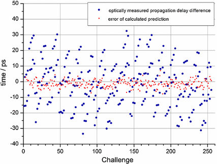
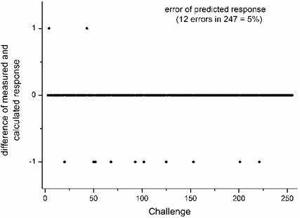
According to the measured values, we can predict the behavior of both chains for all other challenge combinations based on the linear additive model of the arbiter PUF. To prove the applicability of this model, we predicted theoretically the overall delay of both chains for a set of arbitrary challenge combinations and then measured the timings in practice. For instance, the calculated timing difference between both chains for the challenge 00000111 is the sum of measured differences of challenges 00000001, 00000010 and 00000100, which is 7 ps. The measured value is 9 ps, with 2 ps deviation from the predicted value. This example shows that the prediction is accurate enough for this specific challenge; however, it still cannot guarantee the same accuracy for all other possible combinations. Hence, we have measured the delays at the end of both chains for all 255 possible challenges. As it can be found in Fig. 9, the circle dots are showing the optically measured propagation delay differences of both chains from challenge 1 (i.e., 10000000) to challenge 255 (i.e., 11111111). Note that the challenge 0 (i.e., 00000000) is the reference challenge. The square dots show the deviation of the predicted values from the real values, see Fig. 9. As it can be seen, the average of the deviation between the measured and predicted values is meaningfully less than typical delay differences at the end of the chain, which does not affect the response prediction. In order to calculate the precise error rate of response prediction, we compared all predicted responses with the real responses based on optical measurements, see Fig. 10. Out of 247 applied challenges, the response of 12 challenges is predicted incorrectly. Hence, we could obtain the prediction accuracy of 95 %.
6 Discussion
6.1 Feasibility of the Attack
In order to obtain spatial orientation of the PUF circuit by using the CCD detector, the chip has to be thinned. Thinning the silicon substrate from the backside of the chip might change the CRP behavior of the PUF due to the changes in physical properties of the silicon substrate. However, the InGaAs SAPD is still able to detect photons without thinning the substrate. Therefore, only one IC sample has to be thinned, if we aim to apply the same approach on multiple IC samples.
To prevent the semi-invasive attacks, many modern IC architectures utilize the passive and active meshes as well as sensors on the frontside of the IC to detect the attack. By contrast, there is no such protection mechanism on the IC backside, and therefore, this type of attacks cannot be detected from the backside. Furthermore, since our attack is passive and does not require thinning of the silicon substrate, the proposed countermeasures for active fully-invasive attacks, such as 3D hardware architectures [6] and coating PUFs [52], are ineffective. Potential countermeasure against our attack could be an algorithmic mechanism, which prevents the attacker to repeat the same challenge multiple times. In this case, the attacker might not get enough photons for accurate measurement of the delays.
Measuring the effect of each challenge takes approximately 12.5 s, when supplying the chip with 2.2 V and enabling the PUF input with 4 MHz frequency. Supplying the chip with 1.8 V, for example, reduces the number of emitted photons by a factor of 3, and the measurement time increases consequently by a factor of 3. However, we can increase the frequency to 100 MHz to increase the number of emitted photons and to reduce the measurement time. Furthermore, immersion objectives or objective lenses with a larger numerical aperture can be utilized to reduce the measurement time to less than 1 s for each challenge.
Although our experiment was conducted for an 8-bit arbiter PUF, the same delay measurement technique can be applied to arbiter PUFs with higher number of stages. Physical characterization of arbiter PUF, such as modeling attacks, assists the attacker to predict the response to any arbitrary applied challenge. Prediction of responses for unseen challenges enables the attacker to create a CRP lookup table in the software or hardware to emulate the CRP behavior of the arbiter PUF, which is referred to a digital clone. Hence, the unpredictability and unclonability features, which are two of the main requirements of any PUF [24], are not supported anymore. Besides, measurement of the rigorous delay values might enable the attacker to create even a physical clone of the arbiter PUF. To this end, it is possible to have a precise delay map of the LEs on a second platform and try to utilize those, whose delays are close to the stages of the target PUF. Another option, though it is much more expensive, is to edit the circuit delays of the second platform with the help of FIB [40] to obtain timings close to timings of the target arbiter PUF. Thus, although achieving a physical clone of an arbiter PUF is an onerous task, it is theoretically possible.
6.2 Semi-Invasive Attack Versus Modeling Attack
We have to consider two different scenarios to compare our proposed side-channel attack with modeling attacks. In the first scenario, there is no mechanism hiding the challenges and responses, and therefore, the attacker have direct access to CRPs. In the second scenario, nonlinear architecture of PUFs, such as XOR arbiter PUFs [47], hides the response of each arbiter chain from the attacker. Furthermore, the responses can be permuted by employing controlled mechanisms such as hash functions [17].
In the first scenario, in practice the modeling attacks can be very effective, and the number of CRPs required to retrieve the response for an unseen challenge is not enormous [36]. The main advantage of the modeling attacks over our proposed technique is that they are much more cost-effective. Moreover, the semi-invasive attacks require direct physical access to the DUT, while it might not be the case for the modeling attacks. However, in the second scenario, where the responses of the multiple arbiter PUFs are XORed, the effectiveness of modeling attacks is impaired. It has been proved that the pure modeling techniques can break the security of XOR arbiter PUFs with a limited number of arbiter chains [16]. Although combining modeling attacks with side-channel information can relax this theoretical restriction, there still exists a bound on the effectiveness of these attacks [38]. Furthermore, the modeling attacks could be theoretically very weak when the response of the PUF is not available due to mathematically permutation by performing a hash function.
The strength of our proposed semi-invasive attack is revealed in the second scenario, where no electrical access to the responses is available. As our proposed attack measures directly the delays of PUF chains before the arbiter, accessing the generated responses is irrelevant. Therefore, an XOR arbiter PUF can be fully characterized regardless of the number of arbiter chains. It is obvious that the number of required challenges in our approach increases only linearly, when increasing of number of stages. In a similar way, each and every controlled mechanism on the response of the PUF can be bypassed. It has been shown that even when the challenges are controlled, e.g., by performing a hash function, lattice basis reduction attacks can be launched, where the measured delays are the only inputs required to disclose the hidden challenges [13].
6.3 Applicability of the Attack on Smaller Technologies
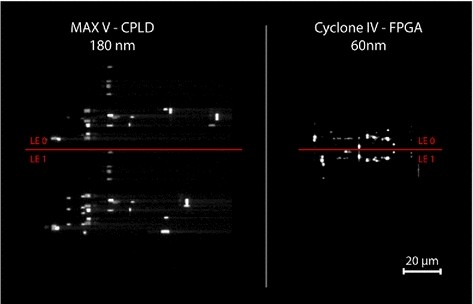
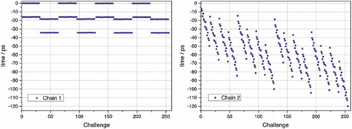
While in our proof-of-concept implementation a CPLD is utilized, the results are directly applicable to arbiter PUFs realized in all classes of CMOS devices, such as FPGAs and application specific integrated circuits (ASICs). However, the emission intensity is reduced by the chips with smaller technologies, due to their lower supply voltage. Moreover, the shrunken transistors might not be clearly distinguishable from each other by conducting spatial photonic emission analysis, and therefore, the PUF stages cannot be identified. The question then arises whether the same spatial photonic emission analysis of arbiter PUFs can be applied on the chips relying on smaller technologies. To answer this question, we have utilized an Altera Cyclone IV FPGA (part number EP4CE6E22C8N) manufactured with 60 nm process [2] as a DUT, see Fig. 11. We chose the Cyclone IV, since it is similar in architecture to the MAX V. This enables us to utilize the same arbiter PUF implementation, which allows us a direct comparison. As the feature size of Cyclone IV is three times smaller than of MAX V, it is expected that the corresponding downscaled size of the LEs results in an intense decrease of the photon emission rate. A comparison of photon emission images of both ICs is shown in Fig. 12. Despite the small feature size of 60 nm adjacent LEs in the Cyclone IV are clearly resolved as well as parts of their inner structure. However, the photon emission rate of the relevant transistors is about ten times lower in Cyclone IV as compared to MAX V, which at least increase the required measurement effort tenfold. In order to estimate the necessary effort, we started with electrical measurements of the propagation delays for each challenge by connecting the electrical output of the last stage of every PUF chain directly to the TDC, see Fig. 3. Electrical measurements are not only simpler and faster but also more accurate. We achieved a timing accuracy of 0.5 ps.
Figure 13 shows the propagation delays of both arbiter PUF chains for each challenge with regard to the propagation delays of reference challenge 0. As can be seen, every stage of chain 2 contributes with a delay difference of about 5–20 ps to the delay of the chain, which is resolvable by optical measurements, whereas in chain 1 only 2 of the 8 stages showed a challenge dependency, which is insufficient for our analysis. Hence, we compared the timings of many LEs of the Cyclone IV to realize a different chain 1 path that has more challenge dependent stages. The analysis of all LEs revealed that the variance of their propagation delays, except a few, is too small for this type of arbiter PUF implementation. As Fig. 13 shows, the derived response of the PUF is dominated by chain 1. Further optical measurements on such a system are pointless until a better implementation of the PUF stages on the FPGAs is found. However, our experiments proved that photon emission still can be used to assess the signal propagation and structural properties of ICs with feature size down to 60 nm and is therefore a powerful tool for a physical characterization of arbiter PUFs.
7 Conclusion
In this work, we demonstrated how photonic emission analysis from the backside of the chip can help us to physically characterize arbiter PUF. The experimental results with minimum number of measurements have shown that the arbiter PUF can be effectively characterized. The comparison between our approach and modeling techniques has shown that our methodology requires far less challenges than modeling attacks. Furthermore, our technique does not require any PUF responses. Although we carried out our experiments on the CPLD PUF implementations, the same methodology can be applied to other hardware implementations. As a result, it is revealed that the timing-based PUFs, specifically arbiter PUFs, are vulnerable to photonic emission analysis.
References
Altera, MAX V Device Handbook (Altera Corporation, San Jose, 2011)
Altera, Cyclone IV Device Handbook (Altera Corporation, San Jose, 2014)
G.T. Becker, The gap between promise and reality: on the insecurity of XOR arbiter PUFs, in Cryptographic Hardware and Embedded Systems—CHES 2015 (Springer, Berlin, 2015), pp. 535–555
G.T. Becker, R. Kumar, Active and passive side-channel attacks on delay based PUF designs. IACR Cryptology ePrint Archive 2014, 287 (2014)
C. Boit, Fundamentals of photon emission (PEM) in silicon—electroluminescence for analysis of electronic circuit and device functionality, in Microelectronics Failure Analysis: Desk Reference (ASM International, New York, 2004), p. 356 ff
S. Briais, S. Caron, J.M. Cioranesco, J.L. Danger, S. Guilley, J.H. Jourdan, A. Milchior, D. Naccache, T. Porteboeuf, 3D Hardware canaries, in Cryptographic Hardware and Embedded Systems—CHES 2012 (Springer, Berlin, 2012) pp. 1–22
J. Delvaux, D. Gu, D. Schellekens, I. Verbauwhede, Secure lightweight entity authentication with strong PUFs: mission impossible?, in Cryptographic Hardware and Embedded Systems—CHES 2014 (Springer, Berlin, 2014), pp. 451–475
J. Delvaux, R. Peeters, D. Gu, I. Verbauwhede, A survey on lightweight entity authentication with strong PUFs. ACM Comput. Surv. 48(2), 26:1–26:42 (2015)
J. Delvaux, I. Verbauwhede, Side channel modeling attacks on 65nm arbiter PUFs exploiting CMOS device noise, in 2013 IEEE International Symposium on Hardware-Oriented Security and Trust (HOST) (IEEE, New York, 2013), pp. 137–142
J. Delvaux, I. Verbauwhede, Fault injection modeling attacks on 65 nm arbiter and RO sum PUFs via environmental changes. Circuits Syst. I Regul. Pap. IEEE Trans. 61(6), 1701–1713 (2014)
J. Di-Battista, J.C. Courrege, B. Rouzeyre, L. Torres, P. Perdu, When failure analysis meets side-channel attacks, in Cryptographic Hardware and Embedded Systems, CHES 2010 (Springer, Berlin, 2010), pp. 188–202
J. Ferrigno, M. Hlaváč, When AES blinks: introducing optical side channel. Inf. Secur. IET 2(3), 94–98 (2008). doi:10.1049/iet-ifs:20080038
F. Ganji, J. Krämer, J.P. Seifert, S. Tajik, Lattice basis reduction attack against physically unclonable functions, in Proceedings of the 22nd ACM SIGSAC Conference on Computer and Communications Security (ACM, New York, 2015), pp. 1070–1080
F. Ganji, S. Tajik, J.P. Seifert, PAC learning of arbiter PUFs, security proofs for embedded systems–PROOFS (2014). https://eprint.iacr.org/2015/378.pdf. Accessed 18 May 2015
F. Ganji, S. Tajik, J.P. Seifert, Let me prove it to you: RO PUFs are provably learnable, in Information Security and Cryptology-ICISC 2015 (Springer, Berlin, 2015)
F. Ganji, S. Tajik, J.P. Seifert, Why attackers win: on the learnability of XOR arbiter PUFs, in Trust and Trustworthy Computing (Springer, Berlin, 2015), pp. 22–39
B. Gassend, D. Clarke, M. Van Dijk, S. Devadas, Controlled physical random functions, in Proceedings of the 18th Annual Computer Security Applications Conference, 2002 (IEEE, New York, 2002) pp. 149–160
B. Gassend, D. Clarke, M. Van Dijk, S. Devadas, Silicon physical random functions, in Proceedings of the 9th ACM Conference on Computer and Communications Security (ACM, New York, 2002), pp. 148–160
C. Helfmeier, C. Boit, D. Nedospasov, J.P. Seifert, Cloning physically unclonable functions, in 2013 IEEE International Symposium on Hardware-Oriented Security and Trust (HOST) (IEEE, New York, 2013), pp. 1–6
C. Helfmeier, C. Boit, D. Nedospasov, S. Tajik, J.P. Seifert, Physical vulnerabilities of physically unclonable functions, in Proceedings of the Conference on Design, Automation & Test in Europe (European Design and Automation Association, Leuven, 2014), p. 350
J. Krämer, D. Nedospasov, A. Schlösser, J.P. Seifert, Differential photonic emission analysis, in Constructive Side-Channel Analysis and Secure Design (Springer, Berlin, 2013), pp. 1–16
J.W. Lee, D. Lim, B. Gassend, G.E. Suh, M. Van Dijk, S. Devadas, A technique to build a secret key in integrated circuits for identification and authentication applications, in VLSI Circuits, 2004. Digest of Technical Papers. 2004 Symposium on (IEEE, New York, 2004), pp. 176–179.
D. Lim, J.W. Lee, B. Gassend, G.E. Suh, M. Van Dijk, S. Devadas, Extracting secret keys from integrated circuits. Very Large Scale Integr. (VLSI) Syst IEEE Trans. 13(10), 1200–1205 (2005)
R. Maes, Physically Unclonable Functions: Constructions, Properties and Applications (Springer, Berlin, 2013)
R. Maes, I. Verbauwhede, Physically unclonable functions: a study on the state of the art and future research directions, in Towards Hardware-Intrinsic Security (Springer, Berlin, 2010), pp. 3–37
M. Majzoobi, F. Koushanfar, S. Devadas, FPGA PUF using programmable delay lines, in 2010 IEEE International Workshop on Information Forensics and Security (WIFS) (IEEE, New York, 2010), pp. 1–6
D. Merli, J. Heyszl, B. Heinz, D. Schuster, F. Stumpf, G. Sigl, Localized electromagnetic analysis of RO PUFs, in 2013 IEEE International Symposium on Hardware-Oriented Security and Trust (HOST) (IEEE, New York, 2013), pp. 19–24
D. Merli, D. Schuster, F. Stumpf, G. Sigl, Semi-invasive EM attack on FPGA RO PUFs and countermeasures, in Proceedings of the Workshop on Embedded Systems Security (ACM, New York, 2011), p. 2
D. Merli, D. Schuster, F. Stumpf, G. Sigl, Side-channel analysis of PUFs and fuzzy extractors, in Trust and Trustworthy Computing (Springer, Berlin, 2011), pp. 33–47
D. Nedospasov, A. Schlösser, J.P. Seifert, S. Orlic, Functional integrated circuit analysis, in 2012 IEEE International Symposium on Hardware-Oriented Security and Trust (HOST) (2012), pp. 102–107
D. Nedospasov, J.P. Seifert, C. Helfmeier, C. Boit, Invasive PUF analysis, in 2013 Workshop on Fault Diagnosis and Tolerance in Cryptography (FDTC) (IEEE, New York, 2013), pp. 30–38
Y. Oren, A.R. Sadeghi, C. Wachsmann, On the effectiveness of the remanence decay side-channel to clone memory-based PUFs, in Cryptographic Hardware and Embedded Systems-CHES 2013 (Springer, Berlin, 2013), pp. 107–125
E. Öztürk, G. Hammouri, B. Sunar, Towards robust low cost authentication for pervasive devices, in Pervasive Computing and Communications, 2008. PerCom 2008. Sixth Annual IEEE International Conference on (IEEE, New York, 2008), pp. 170–178
R. Pappu, B. Recht, J. Taylor, N. Gershenfeld, Physical one-way functions. Science 297(5589), 2026–2030 (2002)
W. Rankl, W. Effing, Smart Card Handbook (4th ed.) (Wiley, Hoboken, 2010)
U. Rührmair, F. Sehnke, J. Sölter, G. Dror, S. Devadas, J. Schmidhuber, Modeling attacks on physical unclonable functions, in Proceedings of the 17th ACM Conference on Computer and Communications Security (ACM, New York, 2010), pp. 237–249
U. Rührmair, J. Sölter, F. Sehnke, On the foundations of physical unclonable functions. IACR Cryptology ePrint Archive 2009, 277 (2009)
U. Rührmair, X. Xu, J. Sölter, A. Mahmoud, M. Majzoobi, F. Koushanfar, W. Burleson, Efficient power and timing side channels for physical unclonable functions, in Cryptographic Hardware and Embedded Systems—CHES 2014 (Springer, Berlin, 2014), pp. 476–492
A.R. Sadeghi, I. Visconti, C. Wachsmann, Enhancing RFID Security and Privacy by Physically Unclonable Functions (Springer, Berlin, 2010)
R. Schlangen, R. Leihkauf, U. Kerst, T. Lundquist, P. Egger, C. Boit, Physical analysis, trimming and editing of nanoscale IC function with backside FIB processing. Microelectron. Reliab. 49(9), 1158–1164 (2009)
A. Schlösser, E. Dietz, S. Frohmann, S. Orlic, Highly resolved spatial and temporal photoemission analysis of integrated circuits. Meas. Sci. Technol. 24(3), 035102 (2013)
A. Schlösser, D. Nedospasov, J. Krämer, S. Orlic, J.P. Seifert, Simple photonic emission analysis of AES, in Cryptographic Hardware and Embedded Systems—CHES 2012 (Springer, Berlin, 2012), pp. 41–57
B. Škorić, P. Tuyls, W. Ophey, Robust key extraction from physical uncloneable functions, in Applied Cryptography and Network Security (Springer, Berlin, 2005), pp. 407–422
S. Skorobogatov, Optical fault masking attacks, in 2010 Workshop on Fault Diagnosis and Tolerance in Cryptography (FDTC) (IEEE, New York, 2010), pp. 23–29
S.P. Skorobogatov, R.J. Anderson, Optical fault induction attacks, in Cryptographic Hardware and Embedded Systems-CHES 2002 (Springer, Berlin, 2003), pp. 2–12
F. Stellari, P. Song, H.A. Ainspan, Functional block extraction for hardware security detection using time-integrated and time-resolved emission measurements, in VLSI Test Symposium (VTS), 2014 IEEE 32nd (IEEE, New York, 2014), pp. 1–6
G.E. Suh, S. Devadas, Physical unclonable functions for device authentication and secret key generation, in Proceedings of the 44th annual Design Automation Conference (ACM, New York, 2007), pp. 9–14
S. Tajik, E. Dietz, S. Frohmann, J.P. Seifert, D. Nedospasov, C. Helfmeier, C. Boit, H. Dittrich, Physical characterization of arbiter PUFs, in Cryptographic Hardware and Embedded Systems—CHES 2014 (Springer, Berlin, 2014), pp. 493–509
S. Tajik, F. Ganji, J.P. Seifert, H. Lohrke, C. Boit, Laser fault attack on physically unclonable functions, in 2015 Workshop on Fault Diagnosis and Tolerance in Cryptography (FDTC) (IEEE, New York, 2015)
S. Tajik, D. Nedospasov, C. Helfmeier, J.P. Seifert, C. Boit, Emission analysis of hardware implementations, in 2014 17th Euromicro Conference on Digital System Design (DSD) (IEEE, New York, 2014), pp. 528–534
P. Tuyls, L. Batina, RFID-tags for anti-counterfeiting, in Topics in Cryptology—CT-RSA 2006 (Springer, Berlin, 2006), pp. 115–131
P. Tuyls, G.J. Schrijen, B. Škorić, J. Van Geloven, N. Verhaegh, R. Wolters, Read-proof hardware from protective coatings, in Cryptographic Hardware and Embedded Systems-CHES 2006 (Springer, Berlin, 2006), pp. 369–383
Acknowledgments
The authors would like to acknowledge the support of the German Federal Ministry of Education and Research in the project Photon FX\(^2\) and the Helmholtz Research School on Security Technologies.
Author information
Authors and Affiliations
Corresponding author
Additional information
Communicated by François-Xavier Standaert.
This paper is an extended version of the [48], presented at CHES 2014. Extra measurements to report the prediction precision of our proposed methodology, experimenting on a smaller technology and further discussion on the provided methodology are the main novelties of this version.
Rights and permissions
About this article
Cite this article
Tajik, S., Dietz, E., Frohmann, S. et al. Photonic Side-Channel Analysis of Arbiter PUFs. J Cryptol 30, 550–571 (2017). https://doi.org/10.1007/s00145-016-9228-6
Received:
Revised:
Published:
Issue Date:
DOI: https://doi.org/10.1007/s00145-016-9228-6


