
Abstract
Electron-excited X-ray microanalysis performed in the scanning electron microscope with energy-dispersive X-ray spectrometry (EDS) is a core technique for characterization of the microstructure of materials. The recent advances in EDS performance with the silicon drift detector (SDD) enable accuracy and precision equivalent to that of the high spectral resolution wavelength-dispersive spectrometer employed on the electron probe microanalyzer platform. SDD-EDS throughput, resolution, and stability provide practical operating conditions for measurement of high-count spectra that form the basis for peak fitting procedures that recover the characteristic peak intensities even for elemental combination where severe peak overlaps occur, such PbS, MoS2, BaTiO3, SrWO4, and WSi2. Accurate analyses are also demonstrated for interferences involving large concentration ratios: a major constituent on a minor constituent (Ba at 0.4299 mass fraction on Ti at 0.0180) and a major constituent on a trace constituent (Ba at 0.2194 on Ce at 0.00407; Si at 0.1145 on Ta at 0.0041). Accurate analyses of low atomic number elements, C, N, O, and F, are demonstrated. Measurement of trace constituents with limits of detection below 0.001 mass fraction (1000 ppm) is possible within a practical measurement time of 500 s.
Introduction
Origins: electron probe microanalysis with wavelength-dispersive spectrometry
Electron-excited X-ray spectrometry for the measurement Query of elemental composition on the microstructural scale has been an important part of the materials characterization arsenal since the invention of the electron probe microanalyzer (EPMA) in 1951 by Castaing [1, 2]. Castaing not only produced the first working EPMA instrument but he also established the framework for the fundamental measurement science of the technique, including the physical basis for a practical quantitative analysis method. For the first two decades of the EPMA technique, the diffraction-based wavelength-dispersive X-ray spectrometer (WDS) was the only practical way to measure the X-ray intensities. Castaing recognized that the complex dependence of the WDS efficiency on photon energy made it impractical to develop a quantification procedure that compared different elements measured at different photon energies. Besides the variable solid angle of the WDS that is dependent on photon energy, four or more diffractors with different d-spacings and scattering efficiencies are needed to satisfy Bragg’s equation over the photon energy range of interest from 100 eV to 10 keV. To overcome this measurement dilemma, Castaing developed the “k-ratio” protocol based on measuring the characteristic X-ray intensity, I, for the same element in the unknown and in a standard of known composition:
The characteristic X-ray peak intensity is corrected for background and measured under identical conditions of beam energy, known dose, and detector efficiency for both unknown and standard. By measuring the same peak under identical conditions, the same efficiency value effectively appears in both the numerator and denominator of Eq. (1) as a multiplier of the intensity, and thus the efficiency quantitatively cancels in the k-ratio.
Castaing further described the basis for the physical calculations that are necessary to convert the suite of k-ratios into mass concentrations, which after substantial further contributions by numerous authors (see Ref. [3] for Heinrich’s detailed account of these developments) take the following form:
where C std is the mass concentration of the element of interest in the standard; and Z, A, F, and c are the “matrix correction factors” that calculate the compositionally dependent interelement effects of electron scattering and energy loss (Z), X-ray self-absorption within the specimen (A), and secondary X-ray emission following self-absorption of the electron-excited characteristic (F) and continuum (c) X-rays. Importantly for the Castaing standards-based k-ratio method, the standards required do not have to closely match the composition of the unknown, which is an enormous advantage when dealing with complicated multi-element unknowns. Suitable standards for the k-ratio measurements include pure elements (e.g., Al, Si, Cr, Fe, Ni, etc.), while stoichiometric compounds can be used for those elements that are not in solid form in a vacuum (e.g., MgO for O), that are highly reactive (e.g., KCl for K and Cl), that deteriorate under electron bombardment (e.g., FeS2 for S), or that have a low melting temperature (e.g., GaP for Ga and P).
The extremely sharp focal properties of the WDS forced EPMA analysts to develop procedures to establish and maintain the critical condition of identical detection efficiency when measuring the separate intensities for the unknown and standards required for Eq. (1) [3]. To place the specimen reproducibly within the narrow spatial range, spanning a few micrometers, over which the WDS had constant X-ray transmission, a fixed-position optical microscope with a shallow depth of focus was incorporated into the EPMA at the coincident focal position for all spectrometers. The condition of the specimen surface was recognized to be another critical requirement [4]. It came to be understood early in the development of EPMA that the specimen had to metallographically polished to a very high degree of surface finish, but not chemically etched. To create contrast in optical metallography, chemical etching typically produces topography through orientation-dependent etch rates in different grains and phases, but even fine-scale topography can influence measured X-ray intensities, especially for low-energy photons. Moreover, in some cases, chemical etching induces changes in the surface/near-surface composition, the principal region that is sampled by electron-excited X-rays, rendering the analytical results unrepresentative of the material being measured.
Throughout the development of quantitative electron-excited X-ray microanalysis, researchers rigorously tested the method by measuring as unknowns carefully selected multi-element materials whose microscopic homogeneity could be first confirmed by EPMA and whose overall composition was measured by independent chemical analysis. The distribution of measured relative errors, defined as
as determined by a mature version of the k-ratio/matrix correction procedure in 1975 is shown in Fig. 1 for WDS measurements of majorFootnote 1 constituents [5]. This distribution can be characterized by a standard deviation of 2.5 % relative, so that approximately 95 % of the analyses fall within the span of ±5 % relative error.

Distribution of relative errors [(measured − true)/true × 100 %] using the k-ratio protocol with WDS measurements and matrix corrections with the NBS ZAF procedure FRAME (1975) [5]. Note that the histogram bins have a width of 1 % relative
Further development: energy-dispersive X-ray spectrometry
The development of semiconductor-based X-ray detection in the 1960s led to the first successful energy-dispersive X-ray spectrometer (EDS) using lithium-compensated silicon [Si(Li)-EDS] operated on an electron-column instrument, an EPMA [6]. As compared to the narrow instantaneous energy range of the WDS, the Si(Li)-EDS provided a view of the entire excited X-ray spectrum from a threshold of approximately 100 eV (modern performance) to the Duane-Hunt limit set by the incident beam energy, up to 20 keV or higher. This wide energy range enabled detection of all elements, with the exception of H and He (modern performance), at every location sampled by the beam, which provided an enormous advantage when dealing with complex microstructures where local segregation can create unexpected compositional variation and where unexpected elements can be localized as inclusions. Comprehensive elemental analysis capability, combined with the relative simplicity of non-focusing line-of-sight detection, the large solid angle of collection which exceeds that of WDS by at least a factor of 10, and the long-term operating stability, resulted in the enthusiastic acceptance of EDS, especially by the rapidly developing scanning electron microscope (SEM) community. The combination of SEM imaging with EDS X-ray microanalysis has given the materials community one of its most powerful microstructural characterization tools [2].
The capability of Si(Li)-EDS to perform quantitative X-ray microanalysis was established soon after its introduction by several members of the microanalysis community, most of whom had extensive WDS quantitative microanalysis experience [7–11]. Thus, the initial EDS implementation of quantitative analysis was based upon their experience with the WDS k-ratio protocol. The EDS could be used in an equivalent manner by measuring the intensities for the unknown and appropriate standards under the same carefully controlled conditions of surface condition (highly polished), beam energy, known dose (beam current × detector live time), beam incidence angle, detector elevation angle (“take-off angle”), and detector efficiency (e.g., constant detector-to-target distance to yield constant detector solid angle). The enormous advantages of the EDS over WDS for analysis were quickly recognized: (1) all elements in the unknown were measured simultaneously minimizing the dose to the specimen; (2) the large solid angle of the EDS relative to WDS further improved efficiency of detection which lowered the necessary dose relative to WDS; and (3) the stability of the EDS meant that the spectra of standards could be archived and recalled as needed. Since the measured EDS spectrum consists of the characteristic X-ray peaks superimposed on the X-ray continuum, various strategies were developed to determine characteristic intensities, including digital filtering for background removal followed by multiple linear least squares (MLLS) fitting and background modeling under the peak window constrained by the continuum intensity measured in energy windows where no peaks occurred [8, 10]. The background-corrected characteristic intensities for the unknown and the standards were used to calculate k-ratios followed by the matrix correction procedure. The k-ratio matrix correction procedure with the Si(Li)-EDS was demonstrated to be capable of achieving relative errors within the WDS distribution for major constituents when the characteristic X-ray peaks did not suffer significant overlap from the peaks of other elements. An example is shown in Table 1 for the Si(Li)-EDS analysis of gold-copper alloys (NIST Standard Reference Material 482) where the observed relative errors range from −1.6 to 1.0 %, falling well within the WDS analysis error distribution of Fig. 1.Footnote 2 Further development of the EDS quantitative microanalysis method enabled accurate analyses when significant peak overlaps occurred providing the intensities of the mutually interfering species were similar.
Typical SEM/EDS microanalysis practice
Despite the level of analytical accuracy demonstrated for the EDS k-ratio/matrix corrections protocol and the availability of this procedure within most commercial implementations of EDS analytical software, modern SEM/EDS microanalysis practice has developed along a different trajectory that minimizes the need for the user’s expertise. As an unintended consequence, EDS microanalysis as performed in the SEM has acquired an unfortunate reputation as a “semi-quantitative” technique. This situation has developed because of three contributing factors: (1) the rise of standardless analysis which now dominates EDS quantitative analysis [14]; (2) the severe effects of specimen geometry on the accuracy of X-ray microanalysis which occur no matter which analytical protocol is followed, standards-based or standardless [15]; and (3) the occasional but significant failures in qualitative analysis, i.e., incorrect elemental identification, which immediately undermines confidence in the method [16–18].
The rise of “standardless” quantitative analysis
By necessity, WDS measures each element in the sample relative to the same element in an appropriate standard to eliminate the need to accurately know the spectrometer efficiency. Because the EDS spectrum provides, in every measurement, the complete photon energy range revealing all characteristic X-ray peaks and the X-ray continuum background, it became attractive to develop an alternative approach for quantitative EDS microanalysis that employed the whole spectrum. The so-called “standardless analysis” method requires only the EDS spectrum of the unknown and eliminates the need to measure standards locally or to specify the electron dose [2, 14]. “Standardless analysis” seeks to provide the necessary standard intensity for the denominator of Eq. (1) for each element in the unknown either by theoretical calculation of X-ray generation and propagation in a pure element target (“first principles” standardless) or by the use of a library of actual standards measured on a well-characterized EDS detector at several beam energies under defined conditions that can be related to the efficiency as a function of photon energy of the local EDS (“remote standards” standardless). The resulting suite of k-ratios is then subjected to the same matrix correction calculations of Eq. (2). Because a true first principles implementation of standardless analysis requires an extensive database of X-ray parameters such as the ionization cross section, X-ray fluorescence yield, X-ray mass absorption coefficient, and others, many of which are poorly known, especially for the L-shell and M-shell X-ray families, the “remote standards” method, which actually anchors the quantitative calculations to a suite of archived experimental measurements, is the basis for the typical modern software implementation.
The performance of a recent commercial version of “standardless analysis” is shown in the error histogram of Fig. 2. While this error distribution appears similar to that of the classic k-ratio protocol with WDS or EDS as shown in Fig. 1, it is in fact much broader, with the errors binned in increments of 5 % relative error, compared to the 1 % relative error increments of Fig. 1. For this particular implementation of standardless analysis, the width of the error range that is necessary to capture 95 % of the analytical results is approximately ±30 % relative. While this level of performance may be adequate for some applications, the prospective user of the analytical results of such a procedure needs to be aware of the inherent limitations imposed by such a wide error distribution. Table 2 provides specific examples of the application of this standardless analysis procedure to the analysis of metal sulfides. While the analytical accuracy achieved for FeS (troilite, a meteoritic mineral) is excellent with relative errors less than ±2 % for S and Fe, the relative errors for the analysis of FeS2 (pyrite), CuS (covellite), ZnS (sphalerite), and PbS (galena) exceed 20 % relative, a level of performance so poor that it would not be possible to properly assign the formula for these compounds from the analyzed mass concentrations.

Distribution of relative errors observed for a commercial implementation of standardless analysis (2013). Note that the histogram bins have a width of 5 % relative
Another often overlooked consequence of using the standardless analysis procedure is the requirement that the calculated concentrations must be internally normalized to a sum of unity. This requirement occurs because the relation of the electron dose and the absolute EDS efficiency of the measured spectrum to the remote standards database is lost so that internal normalization is needed to place the calculated concentration values on a meaningful scale. That the analyzed mass concentration total of all constituents in a standardless analysis equals exactly 1.000 (100 wt%) may seem comforting, but the internal normalization that must occur does in fact represent a loss of critical information. In the standards-based k-ratio/matrix corrections protocol performed with WDS or EDS, the sum of the individual constituents rarely coincides exactly with unity, but tends to vary from 0.98 to 1.02, as shown in the example presented in Table 1, a consequence of the inevitable errors that arise in measuring the characteristic intensities and in calculating the matrix correction factors. Analytical totals outside of this range can occur because of uncontrolled deviations in the experimental conditions between measuring the unknown and standards (e.g., differences in coating thickness or in the thickness of native surface oxides), but a low analytical total may also reveal the presence in the analyzed volume of a previously unrecognized constituent. For example, a region of the specimen that is oxidized rather than metallic will contain oxygen at a concentration from 0.2 to 0.3 mass fraction. The analytical total if oxygen is not considered (either by directly measuring its X-ray intensity and making the appropriate matrix correction calculation or by indirectly calculating oxygen by the method of assumed stoichiometry of the cations) will be 0.7–0.8, significantly below unity, which should trigger the curiosity of a careful analyst to further examine the measured spectrum and discover the oxygen peak. While this may seem a trivial example that even a novice analyst should not miss, in fact as we enter an era in which much of our data are collected under automation, the lack of manual inspection combined with the loss of a meaningful analytical total by the standardless method will result in questionable data appearing in the final results that may be difficult to review after collection and processing. As discussed below, a more frequently encountered source of deviation in the analytical total is the impact of uncontrolled “specimen geometry,” i.e., the effects of size, shape, and local surface inclination on beam electron—specimen interaction and the generation and propagation of X-rays, on the measured X-ray intensities. A “zeroth” level assumption in standards-based and standardless analysis procedures is that the specimen composition is the only factor affecting the X-ray intensities. When the specimen geometry deviates from the ideal flat surface placed at known angles to the incident electron beam and the X-ray spectrometer, very large effects on the X-ray intensities can occur, especially when low-energy and high-energy photons are measured in the same analysis.
Despite these limitations, the simplicity of operation required for standardless analysis, which only requires the analyst to measure the EDS spectrum of the unknown and to specify the beam energy and the X-ray emergence angle, has resulted in its widespread acceptance by the SEM/EDS community. Based on our informal surveys of the field, probably more than 98 % of reported quantitative EDS microanalysis results are obtained with some implementation of standardless analysis. However, the modest analytical performance revealed in Fig. 2 and Table 2 is surely a major contributor to the reputation of SEM/EDS as only achieving “semiquantitative” results, while the internal normalization of all results to unity conveys a false sense of accuracy and confidence.
Specimen geometry effects: we can be our own worst enemies when it comes to performing accurate quantification
When analytical results are automatically normalized, an even more egregious source of large, uncontrolled, and likely unrecognized errors in SEM/EDS microanalysis arises from specimen geometry effects [2]. The line-of-sight acceptance of the EDS spectrometer enables the analyst to record an X-ray spectrum from almost any location where the beam strikes the specimen, which can be a useful feature in qualitatively surveying the complex microstructure of a specimen with complex topography. However, specimen geometry effects such as shape and local surface inclination to the beam can have a profound impact on electron scattering and even more importantly, on the path length along which X-rays must travel to the detector and along which they suffer absorption. These “geometric effects” modify the measured relative elemental intensities in ways that have nothing to do with the composition of the specimen. The physical basis assumed for the matrix correction factors of Eq. (2), which are needed for quantification with both the k-ratio standards protocol and the standardless method, is that the compositional difference between the unknown and the standard(s) is the only factor that affects the measured X-ray intensities. When a quantitative analysis of a topographically irregular specimen is performed following the k-ratio/standards protocol, the analytical total will deviate significantly from unity in response to deviations from the ideal flat, highly polished specimen geometry. However, in the standardless analysis method, the inevitable internal normalization to unity eliminates the important information provided by the analytical total that would reveal the impact of specimen geometry effects.
An example of how serious the impact of specimen geometry can be upon analytical accuracy is illustrated in Figs. 3 and 4 for the analysis of a microscopically homogeneous glass, NIST SRM 470 (K411), the complete composition of which is listed in Table 3. Table 3 also contains the results of a standards-based k-ratio protocol analysis of NIST SRM 470 (K411 glass) prepared in the ideal specimen geometry of a flat, highly polished surface (0.1 µm alumina final polish) with a thin (<10 nm) carbon conductive coating for charge dissipation. The relative errors as compared to the SRM certificate values for the average of 20 analyses range from −1.1 to 1.8 %. Figure 3a shows a plot of the distribution from 20 analyzed locations for the concentrations of magnesium and iron, elements which were chosen because the large difference in their photon energies, 1.254 keV for MgKα, β and 6.400 keV for FeKα, make them differentially sensitive to geometric effects since the low-energy photons of Mg suffer much higher absorption compared to the high-energy photons of FeKα [19]. The cluster of the analyses is seen to be very narrow, with one exception. A reasonable question the analyst might ask is whether this outlier represents an actual deviation in the local composition or arises from some other factor. Upon review of the analyzed locations, the outlier in Fig. 3 was in fact determined to be the consequence of an analysis that was performed in a scratch that remained after final polishing, thus representing a geometric effect rather than a true compositional variation. This surface roughness effect is illustrated for a more severe situation in Fig. 3b, which shows the results from 20 analyses at randomly selected locations on the scratched, irregular surface that remained after polishing with 1 µm diamond particles. The results show both a systematic shift in the apparent concentrations and a broadening in the distribution.

a Analysis of NIST SRM 470 (K411 glass) as a flat, highly polished bulk sample (final polish with 100 nm alumina) using the k-ratio protocol with SDD-EDS measurements and NIST DTSA-II. Plot of Fe (normalized weight percent) vs. Mg (normalized weight percent) for 20 randomly selected analyses. Note the outlier (circled). b Analysis of NIST SRM 470 (K411 glass) as a flat, but slightly scratched bulk sample (scratches remaining after 1 µm diamond polish) using the k-ratio protocol with SDD-EDS measurements and NIST DTSA-II. Plot of Fe (normalized weight percent) vs. Mg (normalized weight percent) for 20 randomly selected analyses

Analysis of NIST SRM 470 (K411 glass) in various geometric forms (flat, polished bulk; scratched surface after 600-grit grinding; shallow surface holes, chips, and shards) using the k-ratio protocol with SDD-EDS measurements and NIST DTSA-II. Plot of Fe (normalized weight percent) vs. Mg (normalized weight percent) [19]
The surface analyzed for the analyses reported in Fig. 3b did not appear to be especially rough when viewed in an SEM image. When the SRM 470 (K411 glass) is prepared in more extreme geometric forms, including the scratched surface that remains after grinding with 600 grit silicon carbide, fracture surfaces, and fragmented particles, and then analyzed following the same k-ratio/standards protocol used for the results in Table 3, the normalized concentrations for magnesium and iron are found to span a much broader range, as shown in Fig. 4 [19]. The range of apparent concentrations obtained from the irregularly shaped specimens is so extreme, spanning nearly an order of magnitude for each constituent, that the results would be of dubious value for most applications that depend on an accurate composition for proper interpretation.
Analysis with the standards-based k-ratio/matrix corrections protocol reveals the impact of geometric effects on X-ray microanalysis through the behavior of the raw analytical total [19]. Figure 5a and b individually plot the normalized magnesium and iron concentrations against the raw analytical total from the k-ratio/standards analysis procedure, showing how well the raw analytical total is correlated with the magnitude of the relative error. This example illustrates well the pitfalls of blindly attempting to quantitatively analyze the EDS spectrum obtained from randomly shaped objects. Because of the inevitable normalization that must occur in the standardless analysis procedure, the important clue that the raw analytical total provides that will identify such dubious analyses is lost. By losing this critical information, standardless analysis enables risky analytical behavior with SEM/EDS which contributes enormously to the dismissal of SEM/EDS as being only “semi-quantitative.” Unless the specimen geometry is carefully controlled, SEM/EDS analysis is subject to errors so broad as to render the compositional results of questionable value for many applications.

Analysis of NIST SRM 470 (K411 glass) in various geometric forms (flat, polished bulk; scratched surface after 600-grit grinding; shallow surface holes, chips, and shards) using the k-ratio protocol with SDD-EDS measurements and NIST DTSA-II: a Mg (normalized weight percent) vs. the raw analytical total (weight percent), including oxygen calculated by assumed stoichiometry [19], b Fe (normalized weight percent) vs. the raw analytical total (weight percent), including oxygen calculated by assumed stoichiometry [19]
Qualitative analysis failures
A separate but extremely significant issue is the reliability of elemental identification in the EDS spectrum. The critical first step of qualitative analysis obviously must be correct if the subsequent quantitative analysis is to have any value at all. Automatic identification of the characteristic peaks in the EDS spectrum is a valuable software tool that has been progressively developed with the rise of computing power and speed. Despite its modern sophistication, however, commercial automatic peak identification procedures have been shown to be vulnerable to occasional failures in the labeling of even the highest intensity peaks that correspond to major constituents, despite the EDS being properly calibrated, operated at a reasonable input count rate, and in the absence of significant peak interferences [16–18]. Examples of failures in identification of major constituent peaks as well as false positive identification of minor/trace constituents are shown in Figs. 6, 7, and 8, which illustrate some of the classic blunders encountered. Commercial implementations of automatic peak identification have been found to vary in their particular vulnerabilities. The specific nature and frequency of mistakes encountered depends on the particular system and the choice of the beam energy, which can provide important redundancy when two families of X-rays can be excited for certain elements, e.g., K- and L-families (Z ≥ 21, Sc) or L- and M-families (Z ≥ 56, Ba). Elemental misidentification typically occurs in a few percent of attempted peak identifications for major constituents, with the frequency of mistakes increasing significantly for minor and trace constituents and especially in cases where peak interference occurs [16–18]. Table 4 lists examples of groups of elements whose characteristic peaks occur sufficiently close in energy that peak identification mistakes have been observed in at least one of the peak identification systems tested.


a Lead, beam energy 20 keV, showing correct identification of the Pb L-family and PbMα,β, but misidentification of PbMζ as WM and PbM2N4 as CdL [16–18]. b NIST glass K230 with Pb as a major constituent, beam energy 20 keV; the Pb M-family is misidentified as SK and TcL, while the Pb L-family is ignored [16–18]
Creating an infallible automatic peak identification procedure is, in fact, an extremely difficult problem, especially at the level of the lower intensity peaks associated with minor and trace constituents. To achieve the most robust and reliable results, the prudent analyst will inspect each tentative elemental assignment that is suggested by the automatic peak identification software and confirm or correct the identification by carefully considering possible alternatives using software tools to explore the database of characteristic X-ray energies. In some circumstances, achieving identification with a high degree of confidence may require adjusting the analytical strategy to collect additional spectral measurements at different beam energies, e.g., decreasing the beam energy to reduce the self-absorption that can occur for certain elements or increasing the beam energy to excite an additional X-ray shell to confirm the presence of an element. For some cases involving major constituents when peak interference occurs, and more frequently for confident identification of minor and trace constituents, it is necessary to apply peak fitting procedures followed by careful inspection of the residual spectrum that remains after tentatively identified peaks are subtracted to reveal any peaks that were previously unrecognized. Thus, a sequential peak identification—peak fitting—residual inspection methodology will provide the strongest basis for establishing a high degree of confidence in the suite of elements that is finally identified.
The new (old) quantitative SEM/EDS X-ray microanalysis
SDD-EDS replaces Si(Li)-EDS
SEM/EDS X-ray microanalysis has undergone a remarkable change with the rapid evolution and deployment of the silicon drift detector energy-dispersive spectrometer (SDD-EDS) [20, 21]. Although the detection physics of the SDD-EDS is the same as the Si(Li)-EDS, the modified structure of the SDD-EDS has greatly improved the performance compared to Si(Li)-EDS:
-
(1)
SDD-EDS operates at approximately −20 °C, which is achieved with Peltier electronic cooling, compared to the −190 °C of the Si(Li)-EDS achieved with a liquid nitrogen cryostat. SDD-EDS can be accommodated more readily on SEM columns, and clusters of SDD detectors can be created, increasing the solid angle of collection while enabling higher throughput with separate processing for each detector in a cluster.
-
(2)
Despite operating at a substantially higher temperature, SDD-EDS achieves equal or better resolution performance.
-
(3)
SDD-EDS operates with a shorter pulse-processing time constant for a given resolution, enabling much higher throughput, by a factor of 10–65 depending on the vendor.
-
(4)
SDD-EDS resolution (peak shape) and calibration (peak stability) are nearly constant over the entire input count rate range, as shown for the Mn K-family in Fig. 9a and the Mn L-family in Fig. 9b. This means that the shape and position of the peak reference necessary for accurate MLLS fitting is constant regardless of variations in the peak count rate ranging from that of a major constituent to that of a trace constituent.
Fig. 9 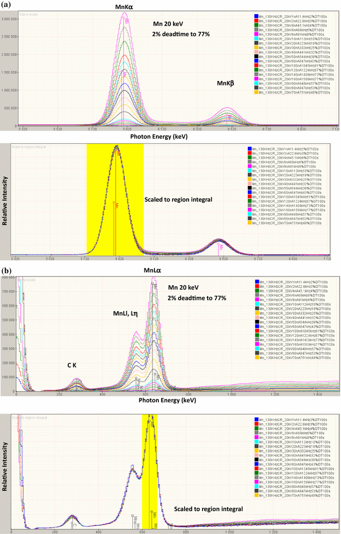
a SDD-EDS (four-detector array) spectra of manganese with a beam energy of E 0 = 20 keV collected over a range of input count rates resulting in deadtime from 2 to 77 % showing the MnKα–MnKβ peak region. Note excellent superposition of the peaks after scaling to the MnKα peak integral. b MnL peak region. Note excellent superposition of the peaks after scaling to the MnLα peak integral
-
(5)
The consistency of performance is such that clusters of SDD detectors can be assembled where the ganged output is not significantly degraded compared to the output of the individual detectors.

SEM/SDD-EDS can provide accurate results
Just as was demonstrated soon after the emergence of the Si(Li)-EDS, SEM/SDD-EDS following the k-ratio protocol can provide accurate results. Table 5 presents the k-ratio protocol analysis of the same spectra of metal sulfides as those reported by standardless analysis in Table 3.
The steps to successful quantitative SEM/SDD-EDS X-ray microanalysis
The results in Table 5 are accurate and fall well within the envelope of relative errors established by EPMA/WDS. However, to achieve this level of performance, it must be recognized that the careful measurement science regime developed for EPMA/WDS must be rigorously followed with SEM/SDD-EDS:
-
(1)
Sample surface condition: The sample must be highly polished to remove topography that creates the geometric effects discussed in Figs. 3, 4, and 5. The resulting highly polished surfaces must not be chemically or electrochemically etched, which can alter the composition of the near-surface region that is actually interrogated in the electron-excited X-ray measurement. Early studies for EPMA/WDS established that final polishing with the finest media then available was necessary to reduce the uncertainty contributed by the remaining specimen topography to an acceptable level for characteristic peaks measured with photon energies above 1 keV [4]. For the low-energy characteristic X-rays below 1 keV needed to measure the elements Be through F, recent Monte Carlo modeling studies indicate that surface scratches must be reduced below a roughness of 50 nm (rms) for a system such as FeO to eliminate differential geometric effects between low-energy and high-energy photon peaks, e.g., O K and FeKα [22].
-
(2)
Non-conducting specimens must be coated with a conducting material which in turn must be connected to a suitable ground to discharge the electron current injected by the beam into the specimen. Typically, a layer of carbon 8–10 nm thick applied by thermal evaporation will suffice for discharging the surface of insulators. Such a coating will have a negligible effect on accuracy for analysis with incident beam energy at 10 keV or higher. For low beam energy analysis, E 0 ≤ 5 keV, differences in the coating thickness between the unknown and the standards can contribute a significant error.
-
(3)
Spectra from the unknowns and standards must be measured under known and reproducible conditions of beam energy, dose (electron current × detector live time), and EDS operating conditions (fixed time constant, which defines a fixed resolution; fixed detector-to-specimen distance which with the detector active area defines the detector solid angle; known detector take-off angle and azimuthal angle relative to the specimen tilt axis; and known specimen tilt, which is preferably zero tilt, i.e., the beam is perpendicular to the specimen surface). A beam current measuring system consisting of a Faraday cup and a digital picoammeter is a necessary component if a fully rigorous k-ratio protocol is to be established [2]. It is highly recommended that a conservative operating strategy be used for SDD-EDS measurements, with the beam current chosen to provide a detector deadtime of approximately 10 % to minimize pulse coincidence (sum peaks). The pulse coincidence problem (discussed in more detail below) is illustrated in Fig. 10, which shows a sequence of SDD-EDS spectra from NIST SRM 470 (K412 glass) which has major peaks arising from the O, Mg, Al, Si, Ca, and Fe constituents. As the beam current is increased to produce an increase in the throughput and consequently the detector deadtime, the in-growth of a complex suite of coincidence peaks can be seen, e.g., combinations of each element such as Al + Al which is frequently misidentified at 2.98 keV as AgL, but also interelement combinations, such as Si + Ca, which at 5.42 keV can be misidentified as CrKα. Coincidence becomes progressively more significant above 15 % deadtime. Thus, by choosing a beam current that yields a deadtime of approximately 10 % on the most highly excited pure element standards such as Al or Si, and then using this beam current for all subsequent measurements, the coincidence problem can be minimized for all recorded spectra. Note that for a pure element of low atomic number, e.g., Al or Si, it is likely that a coincidence peak will still be seen for the primary peak even with this conservative counting strategy, but when such elements appear in the unknown at lower concentration, coincidence is generally reduced to a negligible level.
Fig. 10 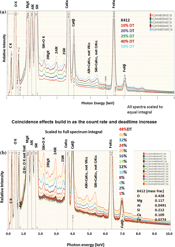
a In-growth of coincidence (sum) peaks: NIST SRM 470 (K412 glass) over a sequence of detector deadtimes, b deadtimes from 1 to 48 %, with all spectra scaled to the full spectrum integral
-
(4)
The stability of the SDD-EDS enables the careful analyst to operate with previously measured and stored standard spectra, providing that a quality assurance protocol is in place to confirm that the current measurement conditions for the unknown are consistent with the conditions under which the archived standards were measured: beam energy, dose, and EDS parameters.
-
(5)
Standards can be co-mounted during metallographic preparation of the unknowns, but a more typical strategy is to prepare a separate standard mount containing a suite of pure elements and stoichiometric compounds. Multi-element mixtures such as alloys glasses, or minerals can also serve as standards, but in addition to accurately knowing the composition, such materials must be confirmed to be homogeneous on a micrometer lateral scale before they can serve as suitable standards.
-
(6)
Commercial vendor software is likely to have an embedded standards-based k-ratio protocol available for the user. For the examples below, all data were collected with vendor software, and the spectra were exported in the open source.msa format (ISO and Microscopy Society of America) that is commonly available on all vendor platforms. Quantitative calculations were performed on these spectra with the NIST DTSA-II EDS software engine [23]. A particular advantage of NIST DTSA-II is the complete report of the analytical error budget that is provided, consisting of the statistical error due to the measurement of the k-ratio propagated through the matrix corrections to provide the equivalent uncertainty in the concentration and the uncertainties in the calculated concentration contributed by the atomic number correction and the absorption correction [24].

SEM/SDD-EDS with MLLS peak fitting can match EPMA/WDS for accuracy and precision in X-ray microanalysis for difficult overlap situations
Comparing WDS and EDS relative intensity measurements (k-ratios)
Most of the examples reported in Table 5 involve the measurement of well-separated characteristic peaks with little overlap, with the exception of PbS, where the Pb M-family interferes with the S K-family. Performing quantitative analysis when severe overlap problems occur, such as for PbS, has traditionally required EPMA/WDS because of the superior spectral resolution of the diffractometer. This situation has now changed with the deployment of SDD-EDS because of the improved throughput and spectrum stability. The performance of SDD-EDS enables routine collection of high-count spectra, e.g., integrated counts from 0.1 keV to E 0 exceeding 5 × 10⁶ collected in 100 s or less while operating with an input count rate that produces a detector deadtime of approximately 10 %. This combination of high-count spectra with stable peak shape and position provides statistically robust peak references needed for MLLS fitting of spectral peaks to accurately extract the characteristic X-ray intensities, including situations in which severe peak overlap occurs, which are the critical input for the k-ratio protocol. Using the NIST DTSA-II EDS software engine to process spectra, it has been demonstrated that SDD-EDS can match WDS for determination of the k-ratio in severe overlap cases, such as that shown in Fig. 11 for the Ba L-family–Ti K-family interference near 4.5 keV [25]. In this study, barium titanate (BaTiO3), benitoite (BaTiSi3O9), and a series of Ba–Ti–Si–O glasses containing various Ba/Ti ratios were measured simultaneously by WDS and SDD-EDS, leading to the observation that the measured k-ratios were statistically indistinguishable, despite a Ba/Ti mass ratio as high as 24:1. Moreover, the SDD-EDS measurement was made with a factor of 3 lower dose (compared to an EPMA equipped with three WDS permitting simultaneous measurement of Ba, Ti, and Si, with the parallel measurements minimizing the WDS dose as much as possible). It is worth noting that the SDD-EDS on this instrument was mounted at a distance of 72 mm to accommodate the three WDS spectrometers that were co-mounted. In a different instrumental configuration designed to optimize the EDS measurement, the SDD-EDS could have been moved to a specimen-to-detector distance of 25 mm, gaining a factor of 10 in solid angle, thus permitting collection of the same spectra with another factor of 10 lower beam current, for an overall dose reduction of a factor of 30 compared to the EPMA with three WDS.

Comparison of the k-ratios measured simultaneously by SDD-EDS (red) and WDS (blue) in barium titantate, benitoite (Ba), and a series of Ba/Ti/Si glasses spanning a mass concentration range as high as Ba:Ti of 24:1 (Color figure online)
Examples of SEM/SDD-EDS applied to challenging analytical problems
The level of peak fitting performance shown in Fig. 11 enables SEM/SDD-EDS to solve analytical problems that were formerly regarded as the exclusive domain of WDS spectrometry, namely those involving characteristic peaks that are close in energy. The peak fitting problems are especially challenging when the constituents have large differences in abundance in the analyzed volume. The following examples demonstrate the capabilities of SEM/SDD-EDS with NIST DTSA-II software carrying out complete analyses, including estimates of the full error budget, in this challenging regime of peak overlaps.
Quantifying major constituents with severely overlapping characteristic X-ray peaks
PbS
The spectrum of PbS (the mineral galena) is shown in Fig. 12 along with the residual spectrum after peak fitting. The principal peak interferences are SKα (2.308 keV) and PbMα (2.346 keV): 38 eV separation; and SKβ (2.468 keV) and PbMβ (2.443 keV): 25 eV separation.

SDD-EDS spectrum of PbS (galena) at a beam energy of E 0 = 10 keV (red); residual spectrum (blue) after peak fitting with CdS and PbSe (Color figure online)
Analytical strategy: a beam energy of 10 keV was chosen to minimize the absorption correction for 2.3 keV photons while providing adequate overvoltage for efficient excitation; references and standards: CuS and PbSe (note that a stoichiometric Pb compound is chosen rather than elemental Pb because the rapid oxidation of metallic Pb creates an uncertain surface composition). The results of the analysis of PbS at 11 locations are presented in Table 6, where atomic concentrations are reported for direct comparison to the ideal formula. Table 6 also contains the results at a single location expressed in mass concentration along with the error budget consisting of the contributions from counting statistics in the determination of the k-ratio and from the estimated uncertainties in the absorption (A) matrix correction and in the atomic number (Z) matrix correction.
MoS2
The SDD-EDS spectrum of MoS2 is shown in Fig. 13 along with the residual spectrum after fitting. The principal interferences are between the SKα (2.307 keV) and MoLα ((2.293 keV) with a separation of 14 eV; SKβ (2.468 keV) and MoLβ1 (2.395) with a separation of 73 eV; and SKβ (2.468 keV) and MoLβ2 (2.518 keV) with a separation of 50 eV.

SDD-EDS spectrum of the MoS2 with E 0 = 10 keV (red); residual spectrum after MLLSQ peak fitting (blue) (Color figure online)
Analytical strategy: A beam energy of 10 keV was chosen to provide adequate overvoltage for efficient excitation. Standards: Elemental Mo served as the standard and fitting reference, and CuS served as the standard and fitting reference for S. Analytical results: The results of the analysis of MoS2 at 7 locations are presented in Table 7, where atomic concentrations are reported for direct comparison to the ideal formula. The analyzed atomic concentrations agree with the ideal formula with a maximum relative error of 0.66 % (Mo). Table 7 also contains the results at a single location expressed in mass concentration along with the components of the error budget.
BaTiO3
The spectrum of BaTiO3 at E 0 = 10 keV is shown in Fig. 14 along with the residual spectrum after peak fitting with BaSi2O5 (the mineral sanbornite) and Ti. The principal peak interferences are BaLα (4.467 keV) and TiKα (4.508 keV): 41 eV separation, and BaLβ3 (4.927 keV) and TiKβ (4.931 keV): 4 eV separation. The analytical results (atomic concentrations) for 15 locations are presented in Table 8, along with a single analyzed location (mass concentration) and the components of the error budget.

SDD-EDS spectrum of BaTiO3 at a beam energy of E 0 = 10 keV (red); residual spectrum (blue) after peak fitting with Ti and BaSi2O5 (sanbornite) (Color figure online)
SrWO4
The spectrum of SrWO4 at E 0 = 10 keV is shown in Fig. 15 along with the residual spectrum after peak fitting with SrF2 and W, with O calculated by assumed stoichiometry. The Sr L- and W M-families create a complex series of interferences: WMα (1.775 keV) and SrLα (1.806 keV): 31 eV separation; SrLα (1.806 keV) and WMβ (1.835 keV): 29 eV separation; and WMβ (1.835 keV) and SrLβ (1.872 keV): 37 eV separation. The analytical results (atomic concentrations) for 15 locations are presented in Table 9, along with a single analyzed location (mass concentration) and the components of the error budget.

SDD-EDS spectrum of SrWO4 at a beam energy of E 0 = 10 keV (red); residual spectrum (blue) after peak fitting with SrF2 and W (Color figure online)
WSi2
The spectrum of WSi2 at E 0 = 10 keV is shown in Fig. 16 along with the residual spectrum after peak fitting with Si and W. The principal interferences are SiK (1.740 keV) and WMα (1.775 keV), 35 eV separation; and SiKβ (1.838 keV) and WMβ (1.835 keV), 3 eV separation. The analytical results (atomic concentrations) for 12 locations are presented in Table 10, along with a single analyzed location (mass concentration) and the components of the error budget.

SDD-EDS spectrum of WSi2 at a beam energy of E 0 = 10 keV (red); residual spectrum (blue) after peak fitting with Si and W (Color figure online)
Quantifying a minor constituent with severe interference from a major constituent
NIST microanalysis glass K2496, the spectrum of which is shown in Fig. 17a and whose composition is listed in Table 11, features the interference of a major constituent Ba (concentration 0.4299 mass fraction) on a minor constituent Ti (concentration 0.0180 mass fraction) with a Ba/Ti mass concentration ratio of 23.9/1. The BaLα and TiKα peaks are separated by 41 eV, while the BaLβ3 and TiKβ peaks are separated by 4 eV. The results of k-ratio protocol analysis of seven replicates with DTSA-II are also presented in Table 11, using elemental Ti and the mineral sanbornite (BaSi2O5) for Si and Ba as references and standards, with O calculated by assumed stoichiometry. After quantification with DTSA-II, the relative errors are less than 2.5 % for all measured constituents.

a SDD-EDS spectrum of NIST microanalysis glass K2496 showing the Ba–Ti region of the spectrum around 4.5 keV (red), and the residual spectrum after fitting for Si, Ba, and Ti (blue). Beam energy 10 keV; dose 1000 nAs; spectrum integral 0.1–10 keV = 12.175 million counts; b The same measured spectrum but with fitting only for Si and Ba (red), revealing the low-level TiKα and TiKβ peaks in the residual spectrum (blue) (Color figure online)
A reasonable question to ask is the following: If the analyst was not aware that Ti was actually present, could this information be discovered during the analytical process? Figure 16a also shows the residual spectrum after peak fitting revealing the nearly featureless background under the composite peaks. Figure 17b demonstrates that when peak fitting is performed without including a peak reference for Ti, the TiKα and TiKβ peaks can be recognized in the residuals. This example illustrates that comprehensive analysis of an unknown must be performed iteratively. In the first round, qualitative analysis first identifies with high confidence the major constituents and any well-resolved minor and trace constituents present. After peak fitting and quantitative analysis for those elements are performed, careful examination of the residual spectrum with those peaks stripped off may reveal previously unrecognized minor and trace constituents hidden under the higher intensity peaks. In the second round, the full analysis is then repeated, including the newly recognized minor/trace constituents. If inspection of the latest residuals reveals no new peaks, the analysis can be considered complete.
The residual spectrum can also be used to estimate limits of detection for trace constituents of interest, and the analytical strategy can be modified if necessary to lower the limit of detection by accumulating more counts.
Quantifying a trace constituent with severe interference from a major constituent
NIST microanalysis glass K873, the spectrum of which is shown in Fig. 18 and whose composition is listed in Table 12, features two examples of interference of a major constituent upon a trace constituent: Ba (concentration 0.219 mass fraction) on Ce (0.0041) (Ba/Ce = 53/1) and Si (0.115) on Ta (0.0041) (Si/Ta = 28/1). The BaLβ1 and CeLα peaks are separated by 12 eV, while the BaLβ2 and CeLβ1 peaks are separated by 106 eV. The SiKα falls between the TaMα (−30 eV) and the TaMβ (26 eV). The results of k-ratio protocol analysis of seven replicates with DTSA-II are also presented in Table 12, using as standards elemental Mn and Ta, with sanbornite (BaSi2O5) for Si and Ba, Al2O3 for Al, CeO2 for Ce, PbTe for Pb, and with O calculated by assumed stoichiometry. The relative errors in the trace constituents are 20 % for Ce and −20 % for Ta, which might be further reduced by accumulating higher counts.

a SDD-EDS spectrum of NIST microanalysis glass K873 (red) and the residual spectrum after fitting for all constituents (blue). Beam energy 15 keV; dose 22500 nAs; spectrum integral 0.1–15 keV = 74.17 million counts. b The same measured spectrum but with fitting excluded for Ta and Ce (red), revealing the low-level Ce L-family and Ta M-family peaks in the residual spectrum (blue) (Color figure online)
Quantitative X-ray microanalysis of low atomic number elements
Quantitative electron-excited X-ray microanalysis of the low atomic number elements, including C, N, O, and F that can only be measured with X-ray peaks whose energies fall below 1 keV, has presented a great challenge since the earliest years of the electron-excited X-ray microanalysis technique [2]. When measured with wavelength-dispersive spectrometry, the low-energy photon peaks are subject to the so-called “chemical effects” manifested as shifts in the X-ray peak position and changes in peak shape that depend on chemical binding. These effects have been described in detail in the classic series of papers by Bastin and Heiligers [26], who developed a “peak-shape” factor correction to compensate for chemical shifts that significantly affected fixed peak-channel WDS measurements. The low-Z spectrum measurement problem is further complicated by peak interferences that often arise from the L-, M-, and N-family X-rays of heavier elements that occur throughout this low photon energy range. Because of the significantly poorer spectral resolution of EDS compared to WDS and the consequent impact of interfering peaks, direct quantitative analysis of light elements by EDS has generally been avoided. For example, when a system is expected to be fully oxidized, which is often the case for ceramics, glasses, and minerals, the oxygen constituent is instead typically calculated by the method of assumed stoichiometry, i.e., the valence of each cation species is assumed, and the amount of oxygen is calculated according to the amount determined for the cation species.
SDD-EDS provides improved measurement sensitivity for photon energies below 1 keV compared to Si(Li)-EDS, and the stable, high-count SDD-EDS spectra can be used to directly measure and quantify the low atomic number elements. The analytical strategy that was employed included selection of a beam energy of 10 keV to provide access to the K-shell X-rays of the transition elements and the L-shell X-rays of higher atomic elements; a beam current to restrict the deadtime to approximately 10 % to minimize coincidence peaks; and a dose to provide spectra with approximately 107 integrated counts. An example of the peak fitting in the low photon energy region (N K and Cr L) for Cr2N is shown in Fig. 19. Quantitative results for several materials containing low atomic number elements are presented in Tables 13 (carbides), 14 (nitrides), 15 (oxides), and 16 (fluorides). The accuracy is adequate to place the results within the ±5 % relative error envelope. The results demonstrate sufficient accuracy to confidently distinguish among compounds with similar amounts of the low atomic number species, e.g., Cr3C2, Cr23C6, and Cr7C3; SiO2 and SiO; and CuO and Cu2O.

SDD-EDS spectrum of Cr2N (red) and residual spectrum (blue) after MLLS fitting: a full spectrum, b expanded to show the low photon energy region (Color figure online)
Limits of detection
Measurement of constituents at the trace level, arbitrarily defined as C < 0.01 mass fraction, requires careful attention to the operating parameters of EDS, particularly the deadtime, which is a measure of the fraction of the real (clock) time during which the detector is occupied processing photons. EDS systems are capable of processing only one photon at a time. Because of the stochastic nature of photon production, when the system is busy processing the charge pulse created by the absorption of a photon in the detector, there exists a finite probability that a second photon will arrive at the detector and distort the measurement of the first photon, creating an artifact measurement consisting of the combination of the photon energies. While any two photons, e.g., characteristic and continuum, can participate in this coincidence process, the noticeable spectral distortions occur for coincidence of two characteristic peak photons (e.g., A + A or A + B), which can create an artifact peak that rises above the continuum background. For the Si(Li)-EDS, which operates with time constants in the range of 25–100 µs for optimum resolution, a pulse inspection function operates which can block such coincidence events that result in the loss of one or both photon events depending on the time spacing. The excluded events lead to a decreasing output count rate as the input count rate increases, eventually paralyzing the process as the deadtime increases to 100 %. At lower deadtime values, the “anti-coincidence” function excludes most artifact coincidence peaks and is typically effective to deadtime limits of approximately 30 % for Si(Li)-EDS. For the much faster SDD-EDS that operates with time constants of a few hundred nanoseconds, pulse inspection is less successful at blocking coincidence events. Figure 10 presents a series of SDD-EDS spectra measured at increasing deadtime from a complex glass with several major constituent peaks that form coincidence peaks in various combinations. For this particular combination of elements, concentrations and detector time constant coincidence becomes visibly significant above 15 % deadtime. The in-growth of coincidence peaks becomes noticeable across large regions of the otherwise featureless background, resulting in numerous artifact peaks, some of which correspond closely in energy to apparent trace constituents, e.g., AlK + CaKα ≈ VKα and SiK + CaKα ≈ CrKα. A conservative count rate that yields a deadtime of approximately 10 % or less is recommended to minimize coincidence artifacts that impact measurements at the trace level. Alternatively, some vendors provide post-acquisition deconvolution based on the observed peak count rates and a statistical model of coincidence.
Even with a conservative counting strategy, SDD-EDS can provide high-count spectra, e.g., integrated spectrum counts >50 million, in practical counting times, e.g., 500 s, that reduce the minimum detectable limit well below a mass concentration of 0.001 (1000 parts per million). Figure 20 shows an example for NIST glasses K496 and K497, which have nearly identical major constituents (O, Mg, Al, and P), while K497 also contains trace levels of a variety of elements. For the purpose of demonstration, the spectrum of K496 can serve as a measure of the continuum background under the measured trace element peaks in K497. The concentration limit of detection, C DL, can be estimated from the measured peak intensity, N S, of a constituent of known or measured concentration, C S, and the intensity of the background under the peak, N B [2]:

SDD-EDS spectrum of NIST microanalysis glasses K496 (blue) and K497 (red) (Color figure online)
For the example shown in Fig. 20, Table 17 presents the C DL for several trace constituents present in K497 as estimated from Eq. (4), all of which are below C = 0.0005 mass fraction (500 ppm).
For analysis of unknowns where the concentrations of trace constituents are returned, the limit of detection can be estimated from this value and the background in the residual spectrum under the trace peak. To estimate the limit of detection for an element not detected, the background in the appropriate portion of the original spectrum (when no interference occurs) or in the residual spectrum after peak fitting (where interference does occur) along with the intensity from a pure element or compound standard spectrum provide the necessary components of Eq. (4).
Summary
SEM/SDD-EDS has reached a level of performance that challenges EPMA/WDS, which is regarded as the “gold standard” of electron-excited X-ray microanalysis, for accuracy and precision even when severe peak interference occurs. Accuracy within ±5 % relative can be routinely achieved for major constituents (mass concentration C > 0.1), even the low atomic number elements, ±10 % relative for minor constituents (0.01 ≤ C ≤ 0.1), and ±25 % relative for trace constituents from 0.001 to 0.01 mass fraction. Limits of detection as low as 0.0005 mass fraction can be achieved for most elements, even when severe peak interference occurs. Remarkably, SEM/SDD-EDS can achieve a given level of precision with a substantially lower dose, by a factor of 10–100, compared to EPMA/WDS, which is a critical issue when beam damage occurs.
However, to achieve SEM/SDD-EDS results at the level of EPMA/WDS, the analyst must be prepared to perform the careful measurement science of the k-ratio protocol, including careful attention to the surface preparation of unknowns and standards, which must be polished to eliminate relief above 50 nm rms. When the specimen deviates from the ideal flat, polished surface set at known angles to the beam and spectrometer, the action of geometric effects, including local surface inclination and thickness, can profoundly affect the accuracy of the analytical results. Since SEM/SDD-EDS can easily image specimens with extreme topography and obtain X-ray spectra from virtually any location that the beam can be placed, there is great temptation to perform quantitative analysis on these spectra, especially since the widespread use of standardless analysis with its inevitable normalization to 100 % hides the obvious effects of specimen topography. As a last cautionary example of the pitfalls of attempting to quantitatively analyze any EDS spectrum that can be recorded in an SEM image, consider the example of a fragment of the mineral pyrite (FeS2) shown in Fig. 21. The relative errors (after normalization to 100 %) and the raw analytical total obtained with the k-ratio protocol and DTSA-II are shown at various locations. While accurate analytical results can be obtained at certain locations in image, at most locations in the images, the deviations from the correct stoichiometry are severe. While the k-ratio protocol and matrix correction provide an important warning flag in the raw analytical total, the standardless analysis procedure would hide this vital clue. The errors inherent in such measurements of topographically rough objects can exceed the ideal flat specimen case by orders of magnitude, so great that the numerical values of elemental concentrations are of dubious value for solving most problems. This paper has sought to demonstrate that it does not have to be this way, and SEM/SDD-EDS can provide extremely credible and valuable analytical results to support advanced materials science providing that the analyst adheres to the k-ratio protocol and matrix corrections performed on a properly prepared flat polished specimen.

Analysis of S and Fe at several locations on a fragment of pyrite, FeS2. The normalized mass concentrations, relative errors, and the raw unnormalized analytical total obtained following k-ratio protocol analyses with NIST DTSA-II (Fe and CuS standards) are indicated at selected locations (Everhart–Thornley detector SEM image)
Notes
Note: in this paper, the following arbitrary convention for broadly classifying the concentration range will be followed:
-
“major,” mass concentration C > 0.1 (more than 10 wt%)
-
“minor” 0.01 ≤ C ≤ 0.1 (1–10 wt%)
-
“trace” C < 0.01 (<1 wt%).
-
Materials analyzed in this paper include NIST Standard Reference Materials, NIST microanalysis research materials (glasses), natural minerals, and stoichiometric compounds confirmed to be homogeneous on a micrometer lateral scale.
References
Castaing R (1951) Application of electron probes to metallographic analysis. Ph.D. Dissertation, University of Paris
Goldstein J, Newbury D, Joy D, Lyman C, Echlin P, Lifshin E, Sawyer L, Michael J (2003) Scanning electron microscopy and X-ray microanalysis, 3rd edn. Springer, New York
Heinrich K (1981) Electron beam X-ray microanalysis. Van Nostrand Reinhold, New York, pp 99–140
Yakowitz H (1968) Evaluation of specimen preparation and the use of standards in electron probe microanalysis. In: Fifty years of progress in metallographic techniques, ASTM-special technical publication 430. American Society of Testing and Materials, Philadelphia 430, pp 383–408
Yakowitz H (1975) Methods of quantitative analysis. In: Goldstein JI, Yakowitz H, Newbury DE, Lifshin E, Colby JW, Coleman JR (eds.) Practical scanning electron microscopy. Plenum, New York, p 338 (error histogram derived from Heinrich K, Yakowitz H, Vieth D (1972) Proceedings of 7th conference electron probe analysis, Microanalysis Society)
Fitzgerald R, Keil K, Heinrich KFJ (1968) Solid-state energy-dispersion spectrometer for electron-microprobe X-ray analysis. Science 528:159–160
Reed SJB, Ware NG (1973) Quantitative electron microprobe analysis using a lithium drifted silicon detector. X-Ray Spectrom 2:69–74
Schamber FC (1973) A new technique for deconvolution of complex X-ray energy spectra. In: Proceedings of 8th national conference on electron probe analysis. Electron Probe Analysis Society of America, New Orleans, p 85
Statham P, Long J, White G, Kandiah K (1974) Quantitative analysis with an energy dispersive detector using a pulsed electron probe and active signal filtering. X-Ray Spectrom 3:153–158
Fiori CE, Myklebust RL, Heinrich KFJ, Yakowitz H (1976) Prediction of continuum intensity in energy-dispersive X-ray microanalysis. Anal Chem 48:172–176
Myklebust R, Fiori C, Heinrich K (1979) FRAME C: a compact procedure for quantitative energy-dispersive electron probe X-ray analysis. National Bureau of Standards Tech. Note 1106 (Spectral processing techniques in a quantitative energy dispersive X-ray microanalysis procedure (FRAME C). In: Heinrich K, Newbury D, Myklebust R, Fiori C (eds) Energy dispersive X-ray spectrometry, U.S. Dept of Commerce, National Bureau of Standards Special Pub. 604 (1981) pp 365–379)
Fiori CE, Swyt CR, Myklebust RL (1992) Desktop spectrum analyzer. Office of standard reference data. National Institute of Standards and Technology, Gaithersburg
Newbury DE (2000) Energy-dispersive spectrometry. In: Kaufmann EN et al (eds) Methods in materials research. Wiley, New York, pp 11d.1.1–11d.1.25 (reissued as EN Kaufmann (ed) (2003) Characterization of materials. ISBN: 0-471-26882-8)
Newbury DE, Swyt CR, Myklebust RL (1995) “Standardless” quantitative electron probe microanalysis with energy-dispersive X-ray spectrometry: is it worth the risk? Anal Chem 67:1866–1871
Newbury DE, Ritchie NWM (2013) Is scanning electron microscopy/energy dispersive spectrometry (SEM/EDS) quantitative? Scanning 35:141–168
Newbury DE (2005) Misidentification of major constituents by automatic qualitative energy dispersive X-ray microanalysis: a problem that threatens the credibility of the analytical community. Microsc Microanal 11:545–561
Newbury DE (2007) Mistakes encountered during automatic peak identification in low beam energy X-ray microanalysis. Scanning 29:137–151
Newbury DE (2009) Mistakes encountered during automatic peak identification of minor and trace constituents in electron-excited energy dispersive X-Ray microanalysis. Scanning 31:1–11
Newbury DE, Ritchie NWM (2011) Is scanning electron microscopy/energy dispersive X-ray spectrometry (SEM/EDS) quantitative? Effects of specimen shape. In: SPIE proceedings, vol 8036, pp 803601-1–803602-16
Struder L, Fiorini C, Gatti E, Hartmann R, Holl P, Krause N, Lechner P, Longoni A, Lutz G, Kemmer J, Meidinger N, Popp M, Soltau H, van Zanthier C (1998) High resolution non dispersive X-ray spectroscopy with state of the art silicon detectors. Mikrochim Acta 15:11–19
Newbury DE (2006) Electron-excited energy dispersive X-ray spectrometry at high speed and at high resolution: silicon drift detectors and microcalorimeters. Microsc Microanal 12:527–537
Newbury DE, Ritchie NWM (2013) Quantitative SEM/EDS, step 1: what constitutes a sufficiently flat specimen? Microsc Microanal 19(Suppl 2):1244–1245
Ritchie NWM, NIST DTSA-II software, including tutorials. www.cstl.nist.gov/div837/837.02/epq/dtsa2/index.html
Ritchie NWM, Newbury DE (2012) Uncertainty estimates for electron probe X-ray microanalysis measurements. Anal Chem 84:9956–9962
Ritchie NWM, Newbury DE, Davis JM (2012) EDS measurements at WDS precision and accuracy using a silicon drift detector. Microsc Microanal 18:892–904
Bastin G, Heijligers H (1991) Quantitative electron probe microanalysis of ultralight elements boron-oxygen. In: Heinrich K, Newbury D (eds) Electron probe quantitation. Plenum, New York, pp 163–175
Disclaimer
Certain commercial equipment, instruments, or materials are identified in this paper to foster understanding. Such identification does not imply recommendation or endorsement by the National Institute of Standards and Technology, nor does it imply that the materials or equipment identified are necessarily the best available for the purpose.
Author information
Authors and Affiliations
Corresponding author
Additional information
Contribution of the United States Government; not subject to U.S. copyright.
Rights and permissions
Open Access This article is licensed under a Creative Commons Attribution 4.0 International License, which permits use, sharing, adaptation, distribution and reproduction in any medium or format, as long as you give appropriate credit to the original author(s) and the source, provide a link to the Creative Commons licence, and indicate if changes were made.
The images or other third party material in this article are included in the article’s Creative Commons licence, unless indicated otherwise in a credit line to the material. If material is not included in the article’s Creative Commons licence and your intended use is not permitted by statutory regulation or exceeds the permitted use, you will need to obtain permission directly from the copyright holder.
To view a copy of this licence, visit https://creativecommons.org/licenses/by/4.0/.
About this article

Cite this article
Newbury, D.E., Ritchie, N.W.M. Performing elemental microanalysis with high accuracy and high precision by scanning electron microscopy/silicon drift detector energy-dispersive X-ray spectrometry (SEM/SDD-EDS). J Mater Sci 50, 493–518 (2015). https://doi.org/10.1007/s10853-014-8685-2
Received:
Accepted:
Published:
Issue Date:
DOI: https://doi.org/10.1007/s10853-014-8685-2