
Abstract
Knowledge of basic circuit analysis
Access this chapter
Tax calculation will be finalised at checkout
Purchases are for personal use only
Author information
Authors and Affiliations
Appendices
Summary
Problems
2.1 13.1 Principle of Operation
13.1.1 Switch Concept
13.1.2 Switch Position in a Circuit
13.1.3 MOSFET Switches
13.1.4 Sketch of Transistor Physics
Problem 13.1
Describe the function and major properties of an electronic switch in your own words.
Problem 13.2
-
A.
Describe the meaning of the ground-side switch , the power-side switch, and the series switch. Why do we distinguish between those switch types?
-
B.
Draw the circuit symbol for a switching NMOS transistor used in the ground-side switch. Draw the circuit symbol for a PMOS transistor used in the power-side switch . Designate the line current direction in both cases.
Problem 13.3
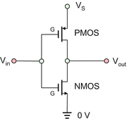
Two digital circuits shown in the following figure operate with a single-supply voltage \( {V}_S=1.8 \mathrm{V} \). The transistor threshold voltages are \( {V}_{\mathrm{Tn}}=\left|{V}_{\mathrm{Tp}}\right|=0.5 \mathrm{V} \), which correspond to a 0.18-μm CMOS process. Note: Every “CMOS process” is a manufacturing process for tiny MOSFETs used in digital circuits. A 0.18-μm CMOS means that the channel length (gate width) of the MOSFET in Fig. 13.5 is greater than or equal to 0.18 μm.

Find the output voltage V out to each circuit if:
-
i.
\( {V}_{\mathrm{in}}=0.0\;\mathrm{V} \)
-
ii.
\( {V}_{\mathrm{in}}=0.2\;\mathrm{V} \)
-
iii.
\( {V}_{\mathrm{in}}=1.6\;\mathrm{V} \)
-
iv.
\( {V}_{\mathrm{in}}=1.8\;\mathrm{V} \)
Problem 13.4
Two digital circuits shown in the figure below operate with a single-supply voltage \( {V}_{\mathrm{S}}=5.0 \mathrm{V} \). The transistor threshold voltages are \( {V}_{\mathrm{Tn}}=\left|{V}_{\mathrm{Tp}}\right|=1.0 \mathrm{V} \).

Find the output voltage V out to each circuit if:
-
i.
\( {V}_{\mathrm{in}}=0.0\;\mathrm{V} \)
-
ii.
\( {V}_{\mathrm{in}}=0.7\;\mathrm{V} \)
-
iii.
\( {V}_{\mathrm{in}}=5\;\mathrm{V} \)
-
iv.
\( {V}_{\mathrm{in}}=4.6\;\mathrm{V} \)
Problem 13.5
For the circuit shown in the figure below, \( {V}_{\mathrm{S}}=2.5 \mathrm{V} \) and \( {V}_{\mathrm{Tn}}=\left|{V}_{\mathrm{Tp}}\right|=0.5 \mathrm{V} \) (0.25-μm CMOS process). Determine the output voltage V out when:
-
A.
\( {V}_{\mathrm{in}}=0.0 \mathrm{V} \)
-
B.
\( {V}_{\mathrm{in}}=0.2 \mathrm{V} \)
-
C.
\( {V}_{\mathrm{in}}=2.3 \mathrm{V} \)
-
D.
\( {V}_{\mathrm{in}}=2.5 \mathrm{V} \)
-
E.
\( {V}_{\mathrm{in}}=1.0 \mathrm{V} \)

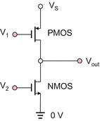
Problem 13.6
For the circuit shown in the figure below, \( {V}_{\mathrm{S}}=2.5 \mathrm{V} \) and \( {V}_{\mathrm{Tn}}=\left|{V}_{\mathrm{Tp}}\right|=0.5 \mathrm{V} \) (0.25-μm CMOS process). Determine the output voltage V out when:
-
A.
\( {V}_1=0.0 \mathrm{V}, {V}_2=0.0 \mathrm{V} \)
-
B.
\( {V}_1=0.7 \mathrm{V}, {V}_2=0.2 \mathrm{V} \)
-
C.
\( {V}_1=2.3 \mathrm{V}, {V}_2=2.3 \mathrm{V} \)
-
D.
\( {V}_1=2.3 \mathrm{V}, {V}_2=0.0 \mathrm{V} \)
-
E.
\( {V}_1=1.0 \mathrm{V}, {V}_2=1.0 \mathrm{V} \)

Problem 13.7
For the circuit shown in the figure below, \( {V}_{\mathrm{S}}=2.5 \mathrm{V} \) and \( {V}_{\mathrm{Tn}}=0.5 \mathrm{V} \). Determine the output voltage V out when:
-
A.
\( {V}_{\mathrm{in}}=0.0 \mathrm{V} \)
-
B.
\( {V}_{\mathrm{in}}=0.2 \mathrm{V} \)
-
C.
\( {V}_{\mathrm{in}}=2.3 \mathrm{V} \)
-
D.
\( {V}_{\mathrm{in}}=2.5 \mathrm{V} \)
The output terminal is disconnected (current cannot flow into this terminal).

Problem 13.8
Draw two alternative circuit symbols for an NMOS switch. Repeat for the PMOS switch.
Problem 13.9
For the circuit shown in the following figure, determine all possible values of the voltage V. The transistor's threshold voltage is 0.5 V.

Problem 13.10
For the circuit shown in the figure below, determine all possible values of the voltage V. The transistor’s threshold voltage is \( \left|{V}_{\mathrm{Tp}}\right|=0.5\mathrm{V} \); the supply voltage is 2.5 V.

Problem 13.11
A circuit shown in the figure below is used to measure the threshold voltage of the NMOS transistor. Could you explain why?
Hint: Determine all possible values of the voltage V.

Problem 13.12
A circuit shown in the figure below is used to measure the threshold voltage of the PMOS transistor. Could you explain why?
Hint: Determine all possible values of the voltage V.

2.2 13.2 Power Switching Circuit
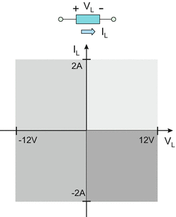
13.2.1 Switching Quadrants
13.2.2 Switching a Resistive Load
Problem 13.13
For a load shown in the figure below, determine the quadrant of operation when:
-
A.
\( {V}_{\mathrm{L}}=-6 \mathrm{V},{I}_{\mathrm{L}}=-1 \mathrm{A} \)
-
B.
\( {V}_{\mathrm{L}}=6 \mathrm{V},{I}_{\mathrm{L}}=1 \mathrm{A} \)
-
C.
\( {V}_{\mathrm{L}}=6 \mathrm{V},{I}_{\mathrm{L}}=-1 \mathrm{A} \)
-
D.
\( {V}_{\mathrm{L}}=-12 \mathrm{V},{I}_{\mathrm{L}}=-2 \mathrm{A} \)

Problem 13.14
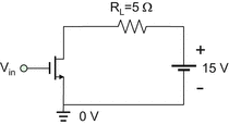
In a switching circuit shown in the figure that follows, an IRF510 n-channel power MOSFET with \( {V}_{\mathrm{Tn}}=3.5 \mathrm{V} \) is used. Assuming zero switch resistance, determine the power delivered to the load when the control voltage is:
-
A.
0 V
-
B.
3 V
-
C.
12 V
-
D.
14 V

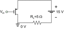
Problem 13.15
In a switching circuit shown in the following figure, a power MOSFET with \( \left|{V}_{\mathrm{Tp}}\right|=3.5 \mathrm{V} \) is used. Assuming zero switch resistance, determine the power delivered to the load when the control voltage V in is
-
A.
0 V
-
B.
2 V
-
C.
15 V
-
D.
12 V

13.2.3 Switching a DC Motor
13.2.4 One-Quadrant Switch for a DC Motor
Problem 13.16
Explain in your own words how switching a motor is different compared to switching a simple resistor load.
Problem 13.17
Explain in your own words the difference between the “free run to a stop” and “brake” states of a DC motor.
Problem 13.18
Prove that a DC motor load operates as a motor (passive load) in quadrants I and III in Fig. 13.8 and as a generator (active load) in quadrants II and IV.
13.2.5 Half H-Bridge for a DC Motor
13.2.6 Full H-Bridge for a DC Motor
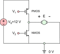
Problem 13.19
For a half H-bridge shown in the following figure, \( {V}_{\mathrm{S}}=12 \mathrm{V} \) and \( {V}_{\mathrm{Tn}}=\left|{V}_{\mathrm{Tp}}\right|=3.5 \mathrm{V} \). The control voltages V 1, V 2 may switch from 0 V to 12 V. Establish the values of two control voltages that ensure the following motor operations:
-
A.
Motor is in forward mode (current direction through the motor is from left to right).
-
B.
Motor suddenly stops (motor terminals are shorted out, which creates the braking effect).
-
C.
Motor runs freely to a stop (motor is disconnected from the power supply).

Problem 13.20
In the half H-bridge circuit shown in the figure to the previous problem, the control voltages V 1, V 2 are either 0 V or 12 V. If we denote the 0-V control voltage by 0 (low) and the 12-V control voltage by 1 (high), all possible combinations of the control voltages are covered by the table that follows (the table in fact lists all binary numbers from 0 to 3). Fill out the table using four states:
-
A.
Forward mode (current direction is from left to right)
-
B.
Brake
-
C.
Free run to a stop
-
D.
Forbidden (short circuit)
V 1 | V 2 | State |
0 | 0 | |
0 | 1 | |
1 | 0 | |
1 | 1 |
Problem 13.21
Suggest and sketch a schematic of the half H-bridge where three switching states (ON, brake, free run to a stop) are realized with only NMOS transistors.
Problem 13.22
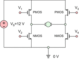
For the H-bridge shown in the following figure, \( {V}_{\mathrm{S}}=12 \mathrm{V} \) and \( {V}_{\mathrm{Tn}}=\left|{V}_{\mathrm{Tp}}\right|=3.5 \mathrm{V} \). The control voltages may switch from 0 V to 12 V. Establish at least one set of particular values for four control voltages V 1, V 2, V 3, V 4 that ensures the following motor operations:
-
A.
Motor is in forward mode (current direction through the motor is from left to right).
-
B.
Motor is in reverse mode (current direction through the motor is from right to left).
-
C.
Motor suddenly stops (motor terminals are shorted out, which creates the braking effect).
-
D.
Motor runs freely to a stop (motor is disconnected from the power supply).

Problem 13.23
In the H-bridge circuit shown in the figure to the previous problem, the control voltages V 1, V 2, V 3, V 4 are either 0 V or 12 V. If we denote the 0-V control voltage by digit 0 (low) and the 12-V control voltage by digit 1 (high), all possible combinations of the control voltages are covered by the table that follows (the table in fact lists all binary numbers from 0 to 15). Fill out the table using five states:
-
A.
Forward mode (current direction is from left to right)
-
B.
Reverse mode (current direction is from right to left)
-
C.
Brake
-
D.
Free run to a stop
-
E.
Forbidden (short circuit)
13.2.7 Application Example: Pulse-Width Modulation (PWM) Motor Controller
Problem 13.24
For a PWM form shown in the following figure, determine:
-
A.
Period, T (show units)
-
B.
Frequency, f (show units)
-
C.
Duty cycle, d (also give its percentage D)
-
D.
Average supply voltage, V DC

Problem 13.25
For a PWM form shown in the following figure, determine
-
A.
Period, T (show units)
-
B.
Frequency, f (show units)
-
C.
Duty cycle, d (also give its percentage D)
-
D.
Average supply voltage, V DC

Problem 13.26*
-
A.
Compile a MATLAB script to generate the figure to Problem 13.24 above. Attach the script and the figure to the homework.
-
B.
Compile two MATLAB scripts to generate the two figures to Problem 13.25 above. Attach the scripts and the figures to the homework.
2.3 13.3 Digital Switching Circuits
13.3.1 NOT Gate or Logic Inverter
13.3.2 NOR Gate and OR Gate
13.3.3 NAND Gate and AND Gate
Problem 13.27
-
A.
Draw the symbol for the logic inverter (NOT gate).
-
B.
Draw the corresponding circuit diagram.
-
C.
Given the input voltage to the NOT gate, fill out the table that follows. The transistors used in the circuit are matched and have equal threshold voltages \( \left|{V}_{\mathrm{Tp}}\right|={V}_{\mathrm{Tn}}=1 \mathrm{V} \).
V in | V out |
0.5 V | |
4.7 V |
Problem 13.28
For the circuit shown in the figure, fill out the table that follows. The transistors used in the circuit are matched and have equal threshold voltages \( \left|{V}_{\mathrm{Tp}}\right|={V}_{\mathrm{Tn}}=1 \mathrm{V} \).

V in | V out |
0 V | |
5 V |
Problem 13.29
For the circuit shown in the figure, fill out the table that follows. The transistors used in the circuit are matched and have equal threshold voltages \( \left|{V}_{\mathrm{Tp}}\right|={V}_{\mathrm{Tn}}=1\mathrm{V} \).

V in | V out |
0.3 V | |
4.2 V |
Problem 13.30
The circuit shown in the following figure is a logic gate. However, it utilizes only one transistor. The current cannot flow into the output terminal (it is disconnected in the figure). Construct:
-
A.
Table of V out versus \( {V}_{\mathrm{in}}=0, 0.5, 4.5, 5 \mathrm{V} \)
-
B.
The truth table
given that the source voltage is 5 V and the threshold voltage is 1 V. What logic gate is it? What value of the resistor R would you choose to minimize circuit loss and the load impact?

Problem 13.31
Repeat the previous problem for the circuit shown in the following figure.

Problem 13.32
Draw the symbol for the logic OR gate and present the corresponding truth table.
Problem 13.33
Draw the symbol for the logic NOR gate and present the corresponding truth table.
Problem 13.34
Draw the circuit diagram:
-
A.
For the NOR gate
-
B.
For the OR gate
Problem 13.35
For the NOR gate with input voltages V 1 and V 2, fill out the table that follows. The transistors used in the circuit are matched and have equal threshold voltages \( \left|{V}_{\mathrm{Tp}}\right|={V}_{\mathrm{Tn}}=1 \mathrm{V} \).
V 1 | V 2 | V out |
0.1 V | 0.7 V | |
0.5 V | 4.9 V | |
4.5 V | 0.1 V | |
4.1 V | 4.4 V |
Problem 13.36
For the OR gate with input voltages V 1 and V 2, fill out the table that follows. The transistors used in the circuit are matched and have equal threshold voltages \( \left|{V}_{\mathrm{Tp}}\right|={V}_{\mathrm{Tn}}=1 \mathrm{V} \).
V 1 | V 2 | V out |
0.3 V | 0.1 V | |
0.2 V | 4.1 V | |
4.1 V | −0.1 V | |
5.3 V | 4.4 V |
Problem 13.37
The following figure is an internal electric circuit of a logic gate. It has three inputs and one output.
-
1.
Fill out the truth table.
-
2.
Draw the symbol of the corresponding logic gate.

Problem 13.38
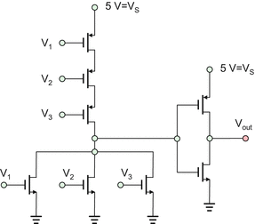
A freshman ECE student attends class if at least one of the following conditions is satisfied:
-
1.
He/she feels that this lecture might be useful.
-
2.
The lecture is not early in the morning.
-
3.
His/her friends might be present there too.
Every morning he/she “votes” by simultaneously pushing any appropriate combination of three 5-V buttons (V 1, V 2, and V 3) placed in parallel. A logic circuit is needed that lights a green LED (outputs 5 V) when there is time to go to the lecture.
-
A.
Draw the corresponding logic circuit in the symbolic form (in the form of logic gates).
-
B.
Draw the MOSFET representation of that logic circuit.
-
C.
Present the corresponding truth table.
Problem 13.39
Draw the symbol for the logic AND gate and present the corresponding truth table.
Problem 13.40
Draw the symbol for the logic NAND gate and present the corresponding truth table.
Problem 13.41
Draw the MOSFET representation
-
A.
For the NAND gate
-
B.
For the AND gate
How many transistors are we using in every case?
Problem 13.42
For the NAND gate with input voltages V 1 and V 2, fill out the table that follows. All transistors used in the circuit are matched and have equal threshold voltages \( \left|{V}_{\mathrm{Tp}}\right|={V}_{\mathrm{Tn}}=1 \mathrm{V} \).
V 1 | V 2 | V out |
0.9 V | 0.9 V | |
0.1 V | 5.1 V | |
4.1 V | −0.1 V | |
4.5 V | 4.7 V |
Problem 13.43
For the AND gate with input voltages V 1 and V 2, fill out the table that follows. The transistors used in the circuit are matched and have equal threshold voltages \( \left|{V}_{\mathrm{Tp}}\right|={V}_{\mathrm{Tn}}=1 \mathrm{V} \).
V 1 | V 2 | V out |
0.1 V | 0.1 V | |
0.2 V | 4.2 V | |
5.1 V | −0.1 V | |
5.0 V | 4.6 V |
Problem 13.44
A senior ECE student attends class if all of the following conditions are satisfied:
-
1.
He/she feels that this lecture might be useful.
-
2.
The lecture is not early in the morning.
-
3.
His/her friends might be present there too.
Every morning he/she “votes” by simultaneously pushing any appropriate combination of three 5-V buttons (V 1, V 2, and V 3) placed in parallel. A logic circuit is needed that lights a green LED (outputs 5 V) when there is time to go to the lecture.
-
A.
Draw the corresponding logic circuit in the symbolic form (in the form of logic gates).
-
B.
Draw the MOSFET representation of that logic circuit.
-
C.
Present the corresponding truth table.
13.3.4 Simple Combinational Logic Circuits. Switching Algebra
13.3.6 Logic Circuit Analysis. Application Example: Logic Gate Motor Controller
13.3.7 Logic Circuit Synthesis
Problem 13.45
Draw a logic circuit with only NAND and NOT gate(s) that realizes an OR gate. Confirm your answer by using the corresponding truth table.
Problem 13.46
Draw a logic circuit with only NAND gate(s) that realizes an OR gate. Confirm your answer by using the corresponding truth table.
Problem 13.47
Draw a logic circuit with only NAND gate(s) that realizes a NOT gate. Confirm your answer by using the corresponding truth table.
Problem 13.48
Four logic circuits shown in the figure below use only the NAND gates. By constructing the truth table for every circuit, establish the equivalence of circuits A,B, C, and D to other logic gates studied in this section.

Problem 13.49
The following figure shows two logic circuits.

Are they equivalent? Prove your answer by constructing the two corresponding truth tables.
Problem 13.50
The following figure shows two logic circuits.

Are they equivalent? Prove your answer by constructing the two corresponding truth tables.
Problem 13.51
Using laws and rules of Boolean algebra, simplify the Boolean expressions
-
A.
\( A\cdot B+A\cdot \left(B+C\right)+B\cdot \left(B+C\right) \)
-
B.
\( \left(A\cdot \overline{B}\cdot \left(C+B\cdot D\right)+\overline{A}\cdot \overline{B}\right)\cdot C \)
Problem 13.52
Using laws and rules of Boolean algebra, simplify the Boolean expressions
-
A.
\( A+\overline{A}\cdot B \)
-
B.
\( \left(A+B\right)\cdot \left(A+C\right) \)
Problem 13.53
The output of the XOR gate is given by \( C=A\cdot \overline{B}+\overline{A}\cdot B \). Using De Morgan’s theorems and laws and rules of Boolean algebra, express the output of the exclusive NOR gate, \( \overline{C} \), in a similar form.
Problem 13.54
If AND gates are substituted in place of NAND gates in the logic circuit in Fig. 13.30c, will the motor controller still function properly? Explain why yes or why no.
Problem 13.55
If NOR gates are substituted in place of NAND gates in the logic circuit in Fig. 13.30c, will the motor controller still function properly? Explain why yes or why no.
Problem 13.56
Given the logic circuit and the input waveforms in the following figure, draw the output waveform on the same figure. Hint: Construct the truth table of the logic circuit first.

Problem 13.57
Given the logic circuit and the input waveforms in the following figure, draw the output waveform on the same figure. Hint: Construct the truth table of the logic circuit first.

Problem 13.58
Given the logic circuit and the input waveforms in the following figure, draw the output waveform on the same figure. Hint: Construct the truth table of the logic circuit first.

Problem 13.59
Given the logic circuit and the input waveforms in the following figure, draw the output waveform on the same figure. Hint: Construct the truth table of the logic circuit first.

Problem 13.60
A small county board is composed of three commissioners. Each commissioner votes on measures presented to the board by pressing a 5-V button indicating whether the commissioner votes for or against a measure. If two or more commissioners vote for a measure, it passes. You are asked to help with a logic circuit that takes the three votes as inputs and lights a green LED (outputs 5 V) to indicate that a measure passed. You can use AND, NAND, and NOT logic gates, as many of them as you need.
-
A.
Present the corresponding logic circuit in the symbolic form (in the form of logic gates).
-
B.
Present the corresponding truth table.
-
C.
How many transistors does your circuit include?
Problem 13.61
A small county board is composed of three commissioners. Each commissioner votes on measures presented to the board by pressing a 5-V button indicating whether the commissioner votes for or against a measure. If two or more commissioners vote for a measure, it passes. You are asked to help with a logic circuit that takes the three votes as inputs and lights a green LED (outputs 5 V) to indicate that a measure passed. You can use OR, NOR, and NOT logic gates, as many of them as you need.
-
A.
Present the corresponding logic circuit in the form of logic gates.
-
B.
Present the corresponding truth table.
-
C.
How many transistors does your circuit include?
13.3.8 The Latch
Problem 13.62
Draw the circuit diagram of a basic latch and explain its operation in your own words.
Problem 13.63
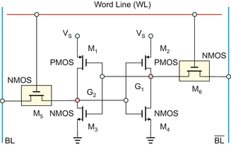
Most of the transistors are used in semiconductor memories. There are several types of semiconductor memories. One of them is the static RAM (SRAM ) or the static random access memory. RAM means that every data bit is accessible any time unlike hard disk memory. SRAM cells provide the fastest operation among all other memories. The figure that follows shows a SRAM memory cell including:
-
1.
The latch with four transistors.
-
2.
A word line WL connected through two access NMOS transistors M 5, M 6. They are always turned on (become the short circuit) when the selected cell’s word line is raised high (to V S or another high voltage).
-
3.
A bit line BL and its counterpart, another bit line \( \overline{\mathrm{BL}} \).

The following figure shows another attempt to design the SRAM memory cell with only four NMOS transistors. Will this design function? Why yes or why no?

Rights and permissions
Copyright information
© 2016 Springer International Publishing Switzerland
About this chapter
Cite this chapter
N. Makarov, S., Ludwig, R., Bitar, S.J. (2016). Switching Circuits. In: Practical Electrical Engineering. Springer, Cham. https://doi.org/10.1007/978-3-319-21173-2_13
Download citation
DOI: https://doi.org/10.1007/978-3-319-21173-2_13
Publisher Name: Springer, Cham
Print ISBN: 978-3-319-21172-5
Online ISBN: 978-3-319-21173-2
eBook Packages: EngineeringEngineering (R0)