
Abstract
We present a review of photonic Network-on-Chip (pNoC) architectures and experimental demonstrations, concluding to the main obstacles that still impede the materialization of these concepts. We also propose the employment of optics in chip-to-chip (C2C) computing architectures rather than on-chip layouts towards reaping their benefits while avoiding technology limitations on the way to many-core set-ups. We identify multisocket boards as the most prominent application area and present recent advances in optically enabled multisocket boards, revealing successful 40 Gb/s transceiver and routing capabilities via integrated photonics. These results indicate the potential to bring energy consumption down by more than 60% compared to current QuickPath Interconnect (QPI) protocol, while turning multisocket architectures into a single-hop low-latency setup for even more than 4 interconnected sockets, which form currently the electronic baseline.
You have full access to this open access chapter, Download conference paper PDF
Keywords
1 Introduction
Workload parallelism and inter-core cooperation are forcing computing to rely at a constantly growing degree on data movement. That led to an upgraded role for the on-chip and off-chip communication infrastructures that support low-power and high-bandwidth interconnect technologies. This came almost simultaneously with the revolutionary advances triggered in the field of optical interconnects [1] and silicon photonics [2]. The last 20 years, optical interconnects were transformed to a mature technology for rack-to-rack [3] and board-to-board communications [4], supporting also the emerging concepts of disaggregated computing [5] and leaf-spine Data Center architectures [6]. However, the on-chip and chip-to-chip photonic technologies are still far away from commercialization, despite the fact that various photonic Network-on-Chip (NoC) architectural concepts have already proposed [7].
In parallel, computing has also experienced some radical advances by turning from simple dual- and quad-core layouts into a highly heterogeneous environment both at chip- and system-level. As shown in Fig. 1, General-Purpose Graphic Processing Units (GP-GPUs) [8] can host more than 4000 CUDA cores on the same die, offering, however, only a 2 Gflop per core processing power. Processing power per core increases in manycore architectures, where up to 1000 cores can be employed [9]. However, when high-performance cores are required as in the case of Chip Multiprocessor (CMP) configurations [10] only a number of up to 32 cores can fit on the same die. The ideal scenario towards boosting processing power would of course imply a die that employs as many cores as a GPU does, but with core capabilities similar to the high-performance cores available in CMPs.

Evolution from single- to many-core computing architectures.
The number of high-performance cores performing as a single computational entity can scale to higher values only through multi-socket designs with 4 or maximum 8 interconnected sockets. The most recent top-class Intel Xeon 8-socket board yields a total number of up to 224 cores [11], requiring, of course, the use of high-bandwidth off-chip inter-socket interconnects. Going one step beyond the multisocket scheme, disintegration of processor dies has been coined in the recent years as a way to form macrochips that will synergize a high amount of high-performance cores, usually exploiting optical inter-die links [12]. This versatile environment at chip-scale suggests a diverse set of requirements that has to be met by optics, depending on the application. However, it creates also a new opportunity to rethink the role of optics in on- and off-chip computing, building upon the proven capabilities of optical hardware towards strengthening the compute architecture/technology co-design perspective.
In this paper, we attempt to investigate the new perspectives for optics in computing, reviewing the high-priority challenges faced currently by the computing industry and evaluating the credentials of state-of-the-art photonics to address them successfully. We provide a review of the work on photonic NoCs, highlighting the bottlenecks towards their materialization. Building on the state-of-art pNoC implementations [13,14,15,16,17,18,19,20,21,22,23,24,25,26,27,28,29,30,31,32,33], we conclude to a solid case for employing integrated photonics in inter-chip multisocket and disintegrated layouts rather than in Network-on-Chip (NoC) implementations, proposing at the same time a flat-topology chip-to-chip multisocket interconnect technology. We demonstrate experimental results for 40 Gb/s multi-socket boards (MSBs) operation, showing the potential to scale to >8-socket designs boosting the number of directly interconnected high-performance cores. Combined with the Hipoλaos Optical Packet Switch (OPS) that has been recently shown to support sub-μsec latencies [34], an optically-enabled rack-scale 256-socket disaggregated setting using a number of 32 interconnected optical 8-socket MSBs, could be implemented, forming in this way a powerful disaggregated rack-scale computing scheme.
The paper is organized as follows: Section 2 outlines the main challenges faced today in the computing landscape, providing also an overview of the research on pNoC architectures, concluding to their main limitations. Section 3 argues for the employment of optics in MSBs and provides experimental results on a 40 Gb/s flat-topology 8-node chip-to-chip (C2C) layout, using O-band integrated photonic transceiver and routing circuitry. Finally, Section 4 concludes the paper.
2 Overview of the PNoC Architectures
In order to define and refine the role of optics in the current computing landscape, it is critical to identify the main challenges currently experienced by the computing industry along the complete hierarchy from on-chip through multi-socket chip-to-chip computational modules. Figure 2 provides an illustrative overview of the main bandwidth, latency and energy needs for different on-chip and off-chip interconnect layers and data transfer operations in a 20 × 20 mm2 processor chip fabricated by a 28 nm Integrated Circuit (IC) CMOS technology.

Energy, bandwidth and latency requirements at different on-chip and off-chip communication needs. The size of every cache memory is bigger for larger capacity caches and their distance from the core is higher as the cache hierarchy increases.
A digital processing operation performed by the core consumes only 20 pJ/bit, but sending data across the chip requires 0.1 pJ/bit for a 1 mm long electrical link, 1 pJ/bit for a 10 mm link and goes up to 4 pJ/bit for a link length of 40 mm. When going off-chip in order to access DRAM, a high amount of 30 pJ/bit is consumed, while a chip-to-chip interconnect link like QPI requires 16.2 pJ/bit. Accessing L1 cache requires 0.2 pJ/bit, while L2 and L3 access requires 1 and 2–4 pJ/bit, respectively. Memory bandwidth reduces with increasing memory hierarchy, with L1 memory bandwidth approaching 20 GB/s and gradually decreasing when going to L2 and L3 access until an upper limit of 12.5 GB/s in the case of DRAM access. Latency follows the inverse path, starting from a high >55 nsec value when fetching from DRAM and gradually reducing with increased memory hierarchy, with L1 access latency being around 1.3 nsec. Having this overview, the main challenges today are formed around:
-
(i)
Interconnect energy consumption: A modern CPU consumes around 1.7 nJ per floating-point operation [35, 36], being 85x higher than the 20 pJ per floating point required for reaching the Exascale milestone within the gross 20 MW power envelope. Current architectures rely to a large degree on data movement, with electronic interconnects forming the main energy consuming factor in both on- and off-die setups [36]. With the energy of a reasonable standard-cell-based, double-precision fused-multiply add (DFMA) being only ~20 pJ, it clearly reveals that fetching operands is much more energy-consuming than computing on them [35, 36].
-
(ii)
Memory bandwidth at an affordable energy envelope: The turn of computing into strongly heterogeneous and parallel settings have transformed memory throughput into a key factor for increasing processing power [35], with the most efficient way for improvement still being the use of wider memory buses and hierarchical caching. However, the highest memory bandwidth per core in modern multicore processors can hardly reach 20 GB/s [37], with L1 cache latency values still being >1 nsec.
-
(iii)
Die area physical constraints: The need to avoid the latency and energy burden of DRAM access has enforced a rich on-chip L1, L2 and L3 cache hierarchy that typically occupies >40% of the chip real-estate [38], suggesting that almost half of the die area is devoted to memory and interconnects instead of processing functions.
-
(iv)
Cache coherency-induced multi- and broadcasting traffic patterns: The need for cache coherency at intra-chip multi- and manycore setups, as well as at inter-chip multisocket systems, yields communication patterns with strong multi- and broadcast characteristics, that have to be satisfied at a low- latency low-energy profile by the interconnect and network-on-chip infrastructure. Multibus ring topologies form a widely adopted multicast-enabling NoC architecture in current modern multi-core processors [39], but still the cache coherency control messages may often account for more than 30% of the total available bandwidth, which may reach even 65% in multisocket settings [40].
The first attempts to exploit photonics for overcoming the on-chip bandwidth, energy and latency bottlenecks mainly inspired by the rapidly growing field of silicon photonics [2]. A number of breakthrough computing architectures relying on pNoC were demonstrated, proposing and utilizing novel silicon photonic transceiver and switching schemes. The pioneering work on photonic Torus [7] was followed by performance and energy advances in pNoC-enabled many-core designs, addressing even cache-coherency needs [41]. All this shaped a promising roadmap for the many-core computing architectures [7, 42,43,44,45,46,47]. At the same time, it revealed the requirements to be met by silicon photonics towards materializing their on-chip employment in practical NoC layouts: transceiver line-rates between 1–40 Gb/s and optoelectronic conversion energies between a few tens to a few hundreds of fJ/bit were considered in the vast majority of pNoC schemes [7, 42,43,44,45,46,47]. Driven by these efforts, photonic integration technology achieved the performance metrics required by pNoC architectures with silicon photonic modulators and SiGe Photo-diodes (PDs) operating at data rates up to 56 Gb/s exhibiting an energy efficiency less than a few tens of fJ/bit [48].
Figure 3 summirizes the most important pNoC and on-chip switches up to now [13,14,15,16,17,18,19,20,21,22,23,24,25,26,27,28,29,30,31,32,33]. Silicon switches have witnessed a remarkable progress yielding high-port connectivity arrangements with a variety of underlying physical mechanisms like the thermo-optic (TO), electro-optic (EO) and opto-mechanical effects [49], allowing for 32 × 32 EO Mach-Zehnder Interferometric (MZI)-based layouts [27], 64 × 64 TO MZI designs [28] and up to 128 × 128 Microelectromechanical switches (MEMS) [33].

Evolution of photonic Network-on-Chip and on-chip photonic switches.
All these demonstrations indicate that integrated photonics can now indeed offer the line-rate, energy, footprint and connectivity credentials required by pNoC-enabled manycore computing architectures. However, the realization of a manycore machine that employs a pNoC layer seems to be still an elusive target, with the main reason being easily revealed when inspecting the non-performance-related co-integration and integration level details of a pNoC-enabled computational setting. Manycore architectures necessitate the on-die integration of a few thousands of photonic structures [7], residing either on 3D integration schemes [50] or on monolithically co-integrated electronic and photonic structures, with transistors and optics being almost at the same layer [51]. However, 3D integration has still not managed to fulfil the great expectations that were raised and is still struggling to overcome a number of significant challenges [52]. On the other hand, monolithic integration has recently accomplished some staggering achievements reporting on real workload execution over an opto-electronic die with optical core-memory interconnection [51]. Nevertheless, this technology has still a long-way to go until reaching the complexity and functionality level required by a many-core pNoC design.
With almost the complete Photonic Integrated Circuit (PIC) technology toolkit being today available as discrete photonic chips, computing can reap the benefits of optics by employing photonics for off-die communication in (i) multisocket and (ii) disintegrated layouts. Both schemes can yield a high number of directly interconnected high-performance cores, unleashing solutions that cannot be met by electronics. At the same time, this approach is fully inline with the 2.5D integration scheme that employs discrete photonic and electronic chips on the same silicon interposer and has made tremendous progress in the recent years [53]. To this end, the employment of off-die communications via discrete photonic chips can form a viable near-term roadmap for the exploitation of photons in computational settings.
3 Optics for Multi-socket Boards
MSB systems rely currently on electrically interconnected sockets and can be classified in two categories:
-
(i)
“glueless” configurations, where point-to-point (P2P) interconnects like Intel’s QPI [54] can offer high-speed, low-latency, any-to-any C2C communication for a number of 4 or 8 sockets. A 4-socket setup can yield a cache-coherent layout with directly interconnected sockets and latency values that range between 60–240 nsec. Scaling to 8-socket designs can only be met through dual-hop links, degrading latency performance but still comprising a very powerful cache-coherent computational setting: Intel’s Xeon E7-8800 v4 was the first processor supporting 8-socket configurations and was by that time advertized as being suitable to “dominate the world” [55]. Figure 4(a) depicts a 4-socket (4S) and 8-socket (8S) layout, respectively, along with their respective interconnects. A typical interconnect like Intel’s QPI operates at a 9.6 Gb/s line-rate and consumes 16.2 pJ/bit, while the total bandwidth communicated by every socket towards all three possible directions is 38.4 GB/s, i.e. 307.2 Gb/s [56].
Fig. 4. 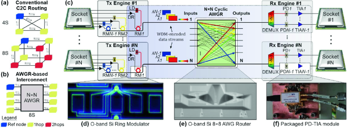
(a) C2C routing in current electronic 4S and 8S MSBs, (b) Flat-topology 8S layout using AWGR-based routing, (c) proposed N × N AWGR-based optical C2C interconnect for MSB connectivity. Photonic integrated circuits employed as the basic building blocks in the 40 Gb/s experimental demonstration: (d) Ring Modulator, (e) 8 × 8 cyclic-frequency AWGR and (f) PD-TIA module. (blue-highlighted areas: part of the architecture demonstrated experimentally, white-highlighted areas: basic building blocks used for the demonstration).
-
(ii)
“glued” configurations, where scaling beyond 8-socket layouts is accomplished by exploiting active switch-based setups, such as PCI-Express switches, in order to interconnect multiple 4- or 8-socket QPI “islands” [56].

With latency and bandwidth comprising the main performance criteria in releasing powerful MSB configurations, “glueless” layouts offer a clear latency-advantage over the “glued” counterparts avoiding by default the use of any intermediate switch. Photonics can have a critical role in transforming “glued” into “glueless” architectures even when the number of interconnected sockets is higher than 8, enabling single-hop configurations, with Fig. 4(b) illustrating how the basic flat-topology can be accomplished for the case of an 8-Socket layout. This has been initially conceived and proposed by UC Davis in their pioneering work on Flat-Topology computing architectures [57] via Arrayed Waveguide Grating Router (AWGR) interconnects, utilizing low-latency, non-blocking and all-to-all optical connectivity credentials enabled by their cyclic-routing wavelength properties. UC Davis demonstrated via gem5 simulations the significant execution time and energy savings accomplished over the electronic baseline [57], revealing also additional benefits when employing bit- parallel transmission and flexible bandwidth-allocation techniques. Experimental demonstrations of AWGR-based interconnection for compute node architectures were, however, constrained so far in the C-band regime, limiting their compatibility with electro-optic Printed Circuit Board (PCB) technology that typically offers a low waveguide loss figure at the O-band [58]. As such, AWGR-based experimental compute node interconnect findings were reported so far only in pNoC architectural approaches, using a rather small line-rate operation of 0.3 Gb/s [18].
The European H2020 project ICT-STREAMS is currently attempting to deploy the necessary silicon photonic and electro-optical PCB technology toolkit for realizing the AWGR-based MSB interconnect benefits in the O-band and at data rates up to 50 Gb/s [59]. It aims to exploit wavelength division multiplexing (WDM) Silicon photonics transceiver technology at the chip edge as the socket interface and a board-pluggable O-band silicon-based AWGR as the passive routing element, as shown in a generic N-socket architecture depicted in Fig. 4(c). Each socket is electrically connected to a WDM-enabled Tx optical engine equipped with N-1 laser diodes (LD), each one operating at a different wavelength. Every LD feeds a different Ring Modulator (RM) to imprint the electrical data sent from the socket to each one of the N-1 wavelengths, so that the Tx engine comprises finally N-1 RMs along with their respective RM drivers (DR). All RMs are implemented on the same optical bus to produce the WDM-encoded data stream of each socket. The data generated by each socket enters the input port of the AWGR and is forwarded to the respective destination output that is dictated by the carrier wavelength and the cyclic-frequency routing properties of the AWGR [57]. In this way, every socket can forward data to any of the remaining 7 sockets by simply modulating its electrical data onto a different wavelength via the respective RM, allowing direct single-hop communication between all sockets through passive routing. At every Rx engine, the incoming WDM-encoded data stream gets demultiplexed with a 1:(N-1) optical demultiplexer (DEMUX), so that every wavelength is received by a PD. Each PD is connected to a transimpedance amplifier (TIA) that provides the socket with the respective electrical signaling.
The AWGR-based interconnect scheme requires a higher number of transceivers compared to any intermediate switch solution, but this is exactly the feature that allows to combine WDM with AWGR’s cyclic frequency characteristics towards enabling single-hop communication and retaining the lowest possible latency. Utilizing an 8 × 8 AWGR, the optically-enabled MSB can allow single-hop all-to-all interconnection between 8 sockets, while scaling the AWGR to 16 × 16 layouts can yield single-hop communication even between 16 sockets, effectively turning current “glued” into “glueless” designs. The ICT-STREAMS on-board MSB aims to incorporate 50 GHz single-mode O-band electro-optical PCBs [60], relying on the adiabatic coupling approach between silicon and polymer waveguides [61] for low-loss interfacing of the Silicon-Photonics (Si-Pho) transceiver and AWGR chips with the EO-PCB.
Next, the first 40 Gb/s experimental results of demonstration with the fiber-interconnected integrated photonic building blocks is presented, extending the recently presented operation of the 8-socket architecture at 25 Gb/s [62]. The main integrated transmitter, receiver and routing building blocks that were used, comprise three discrete chips, i.e. a Si-based RM [48], a Si-based 8 × 8 AWGR routing platform [63] and a co-packaged PD-TIA [64], which are depicted in Fig. 4(d), (e) and (f), respectively. The silicon O-band carrier-depletion micro-ring modulator is an all-pass ring resonator fabricated on imec’s active platform with demonstrated 50 Gb/s modulation capabilities [48]. The RM can be combined with a recently developed low-power driver [65], leading to an energy efficiency of 1 pJ/bit at 40 Gb/s. For the routing platform, the demonstration relied on an O-band integrated silicon photonic 8 × 8 AWGR device [63] with 10 nm-channel spacing, a maximum channel loss non-uniformity of 3.5 dB and a channel crosstalk of 11 dB. Finally, the Rx engine employed a co-packaged uni-traveling InGaAs-InP PIN photodiode (PD) connected with a low-power TIA implemented in 0.13 μm SiGe BiCMOS [64]. The PD-TIA energy efficiency for operation at 40 Gb/s is 3.95 pJ/bit.
The energy efficiency of the proposed 40 Gb/s chip-to-chip (C2C) photonic link is estimated at 5.95 pJ/bit, assuming a 10% wall-plug efficiency for the external laser. This indicates that the proposed architecture has the credentials to lead to 63.3% reduction in energy compared to the 16.2 pJ/bit link energy efficiency of Intel QPI [56]. Figure 5 (a)–(h) show the eye diagrams of the signal at the 8 outputs of the AWGR coressponding to the 8 routing scenarios for all possible input-output port combination, indicating clear eye openings and successful routing at 40 Gb/s with ER values of 4.38 ± 0.31 dB and AM values of 2.3 ± 0.3 dB, respectively. The RM was electrically driven with a peak-to-peak voltage of 2.6 Vpp, while the applied reverse DC bias voltage was −2.5 V. The optical power of the CW signal injected at the RM input was 8 dBm, with the modulated data signal obtained at the RM output having an average optical power level of −6.3 dBm.

Eye diagrams (a)–(h) after routing via the respective In#iOut#j I/O ports of the AWGR.
Going a step further, the proposed optically-enabled MSBs can be beneficially employed in rack-scale disaggregated systems when equipped with an additional transceiver lane for dealing with the off-board traffic and are combined with the recently demonstrated Hipoλaos high-port switch architecture [34]. Recently in [66], it was shown that rack-scale disaggregation among a 256-node system can be successfully accomplished for a variety of communication patterns with an ultra-low mean latency value of <335 nsec for 10 Gb/s data rates. The disaggregated architecture are expected to improve drastically when scaling Hipoλaos data-rates to 40 Gb/s, making this compatible with the 40 Gb/s silicon photonic transmitter reported in this paper.
4 Conclusion
We reviewed the pNoC-enabled manycore architectures proposed over the last decade. After analyzing the co-integration aspects as the main limitation for the realization of pNoC-based computing, we have defined a new role for photonics in the landscape of computing related to off-die communication. We discussed how optics can yield single-hop low-latency multisocket boards for even more than 4 interconnected sockets, demonstrating experimental results for 40 Gb/s C2C interconnection in a 8-node setup via integrated photonic transmitter and routing circuits. Combining 8-socket optical boards with a Hipoλaos optical packet switch shown in [34], photonics can yield a powerful 256-node compute disaggregated system with latency below the sub-μs threshold considered for memory disaggregation environments.
References
Bergman, K.: Photonic networks for intra-chip, inter-chip, and box-to-box interconnects in high performance computing. In: European Conference on Optical Communication (ECOC), Cannes, France (2006)
Lipson, M.: Guiding, modulating, and emitting light on Silicon-challenges and opportunities. J. Lightw. Techn. 23(12), 4222–4238 (2005)
Intel SiP 100G PSM4 Optical Tx. https://www.intel.com/content/www/us/en/architecture-and-technology/silicon-photonics/optical-transceiver-100g-psm4-qsfp28-brief.html. Accessed 12 Apr 2019
Luxtera 2x100G-PSM4 OptoPHY Product Family. http://www.luxtera.com/embedded-optics/. Accessed 12 Apr 2019
Zervas, N.G., Yuan, H., Saljoghei, A., Chen, Q., Mishra, V.: Optically disaggregated data centers with minimal remote memory latency: technologies, architectures, and resource allocation. J. Opt. Commun. Netw. 10(2), A270–A285 (2018)
Bielski, M., et al.: dReDBox: materializing a full-stack rack-scale system prototype of a next-generation disaggregated datacenter. In: 2018 Design, Automation & Test Conference & Exhibition (DATE) (2018)
Shacham, A., Bergman, K., Carloni, L.: Photonic networks-on-chip for future generations of chip multiprocessors. Trans. Comput. 57(9), 1246–1260 (2008)
Kider, J., NVIDIA Fermi architecture. http://www.seas.upenn.edu/~cis565/Lectures2011/Lecture16_Fermi.pdf. Accessed 12 Apr 2019
Bohnenstiehl, B., et al.: KiloCore: a 32-nm 1000-Processor computational array. IEEE J. Solid State Circ. 52(4), 891–902 (2017)
Intel Xeon Platinum 8180 Processor. https://ark.intel.com/products/120496. Accessed 12 Apr 2019
Supermicro Super Server 7089P-TR4T. www.supermicro.com/products/system/7U/7089/SYS-7089P-TR4T.cfm. Accessed 12 Apr 2019
Raj, K., et al.: “Macrochip” computer systems enabled by silicon photonic interconnects. In: Optoelectronic Interconnects and Component Integration IX (2010)
Sherwood-Droz, N., et al.: Optical 4 × 4 hitless slicon router for optical networks-on-chip (NoC). Opt. Express 16(20), 15915 (2008)
Jia, H., et al.: Four-port optical switch for fat-tree photonic network-on-chip. J. Lightw. Technol. 35(15), 3237–3241 (2017)
Yang, L., et. al.: Optical routers with ultra-low power consumption for photonic networks-on-chip. In: Proceedings Conference on Lasers and Electro-Optics (CLEO), San Jose, CA (2012)
Fan, G., Orobtchouk, R., Han, B., Li, Y., Li, H.: 8 × 8 wavelength router of optical network on chip. Opt. Express 25(20), 23677 (2017)
Zhang, C., Zhang, S., Peters, J., Bowers, J.: 8 × 8 × 40 Gbps fully integrated silicon photonic network on chip. Optica 3(7), 785 (2016)
Yu, R., et al.: A scalable silicon photonic chip-scale optical switch for high performance computing systems. Opt. Express 21(26), 32655 (2013)
Testa, F., et al.: Design and implementation of an integrated reconfigurable silicon photonics switch matrix in IRIS project. J. Sel. Topics Quant. Electr. 22(6), 155–168 (2016)
Dong, P., et al.: Reconfigurable 100 Gb/s silicon photonic network-on-chip. In: Proceedings of Optical Fiber Communication Conference (OFC) (2014)
Gambini, F., et al.: Experimental demonstration of a 24-port packaged multi-microring network-on-chip in silicon photonic platform. Opt. Express 25(18), 22004 (2017)
Yang, M., et al.: Non-Blocking 4 × 4 electro-optic silicon switch for on-chip photonic networks. Opt. Express 19(1), 47 (2010)
Lee, B., et al.: Monolithic silicon integration of scaled photonic switch fabrics, CMOS logic, and device driver circuits. J. Lightw. Technol. 32(4), 743–751 (2014)
Hu, T., et al.: Wavelength-selective 4 × 4 nonblocking silicon optical router for networks-on-chip. Opt. Lett. 36(23), 4710 (2011)
Dupuis, N., et al.: Nanosecond-scale Mach-Zehnder-based CMOS photonic switch fabrics. J. Lightw. Technol. 35, 1 (2016)
Dumais, P., et al.: Silicon photonic switch subsystem with 900 monolithically integrated calibration photodiodes and 64-fiber package. J. Lightw. Technol. 36(2), 233–238 (2018)
Qiao, L., Tang, W., Chu, T.: 32 × 32 silicon electro-optic switch with built-in monitors and balanced-status units. Sci. Rep. 7(1), 1 (2017)
Qiao, L., Tang, W., Chu, T.: Ultra-large-scale silicon optical switches. In: Proceedings 2016 IEEE International Conference on Group IV Photonics (GFP), Shanghai (2016)
Seok, T.J.: 64 × 64 Low-loss and broadband digital silicon photonic MEMS switches. In: Proceedings European Conference on Optical Communication (ECOC), Valencia (2015)
Tanizawa, K., et al.: Ultra-compact 32 × 32 strictly-non-blocking Si-wire optical switch with fan-out LGA interposer. Opt. Express 23(13), 17599 (2015)
Lu, L., et al.: 16 × 16 non-blocking silicon optical switch based on electro-optic Mach-Zehnder interferometers. Opt. Express 24(9), 9295 (2016)
Papaioannou, S., et al.: Active plasmonics in WDM traffic switching applications. Sci. Rep. 2(1), 652 (2012)
Kwon, K., et al.: 128 × 128 silicon photonic MEMS switch with scalable row/column addressing. In: Proceedings Conference on Lasers and Electro-Optics (2018)
Terzenidis, N., Moralis-Pegios, M., Mourgias-Alexandris, G., Vyrsokinos, K., Pleros, N.: High-port low-latency optical switch architecture with optical feed-forward buffering for 256-node disaggregated data centers. Opt. Express 26, 8756–8766 (2018)
Parker, S.: The evolution of GPU accelerated computing. In: Proceedings Extreme Scale Computing, IL, USA, 29 July 2013
Dally, B.: Challenges for future computing systems. In: Proceedings HiPEAC 2015, Amsterdam, NL (2015)
Saini, S., et al.: Performance evaluation of the intel sandy bridge based NASA pleiades using scientific and engineering applications. NAS Technical Report: NAS-2015-05
Borkar, S., Chien, A.A.: The future of microprocessors. Commun. ACM 54(5), 67–77 (2011)
Kumashikar, M., Bendi, S., Nimmagadda, S., Deka, A., Agarwal, A.: 14 nm broadwell Xeon® processor family: design methodologies and optimizations. In: Proceedings 2017 IEEE Asian Solid-State Circuits Conference (A-SSCC) (2017)
Bull, S.A.S.: An efficient server architecture for the virtualization of business-critical applications. White paper 2012. https://docuri.com/download/bullion-efficient-server-architecture-for-virtualization_59c1dc51f581710b28689168_pdf. Accessed 12 Apr 2019
Kurian, G., et al.: ATAC. In: International Conference on Parallel Architectures and Compilation techniques - PACT 2010 (2010)
Chen, C., Joshi, A.: Runtime management of laser power in silicon-photonic multibus NoC architecture. J. Sel. Top. Quant. Electr. 19(2), 3700713–3700713 (2013)
Li, Z., Qouneh, A., Joshi, M., Zhang, W., Fu, X., Li, T.: Aurora: a cross-layer solution for thermally resilient photonic network-on-chip. Trans. VLSI Syst. 23(1), 170–183 (2015)
Bahirat, S., Pasricha, S.: METEOR. ACM Trans. Embed. Comput. Syst. 13(3), 1–33 (2014)
Wang, X., Gu, H., Yang, Y., Wang, K., Hao, Q.: RPNoC: a ring-based packet-switched optical network-on-chip. Photonics Technol. Lett. 27(4), 423–426 (2015)
Gu, H., Chen, K., Yang, Y., Chen, Z., Zhang, B.: MRONoC: a low latency and energy efficient on chip optical interconnect architecture. Photonics J. 9(1), 1–12 (2017)
Werner, S., Navaridas, J., Luján, M.: Efficient sharing of optical resources in low-power optical networks-on-chip. J. Opt. Commun. Netw. 9(5), 364–374 (2017)
Pantouvaki, M., et al.: Active components for 50 Gb/s NRZ-OOK optical interconnects in a silicon photonics platform. J. Lightw. Technolo. 35(4), 631–638 (2017)
Lee, B.: Silicon photonic switching: technology and architecture. In: 2017 European Conference on Optical Communication (2017)
Yoo, S.J.B., Guan, B., Scott, R.: Heterogeneous 2D/3D photonic integrated microsystems. Microsyst. Nanoeng. 2(1), 16030 (2016)
Sun, C., et al.: Single-chip microprocessor that communicates directly using light. Nature 528(7583), 534–538 (2015)
Li, C., et al.: Chip scale 12-channel 10 Gb/s optical transmitter and receiver subassemblies based on wet etched silicon interposer. J. Lightw. Technol. 35(15), 3229–3236 (2017)
Zhang, X., et al.: Heterogeneous 25D integration on through silicon interposer. Appl. Phys. Rev. 2(2), 021308 (2015)
Intel: An Introduction to the Intel QuickPath Interconnect. https://www.intel.com/content/www/us/en/io/quickpath-technology/quick-path-interconnect-introduction-paper.html. Accessed 12 Apr 2019
Intel: Intel® Xeon® Processor E7-8800/4800/2800 Families. https://www.intel.com/content/www/us/en/processors/xeon/xeon-e7-8800-4800-2800-families-vol-2-datasheet.html. Accessed 12 Apr 2019
Maddox, R., Singh, G., Safranek, R.: Weaving High Performance Multiprocessor Fabric. Intel Press, Hillsboro (2009)
Grani, P., Proietti, R., Cheung, S., Yoo, S.J.B.: Flat-topology high-throughput compute node with AWGR-based optical-interconnects. J. Lightw. Technol. 34(12), 2959–2968 (2016)
Sugama, A., Kawaguchi, K., Nishizawa, M., Muranaka, H., Arakawa, Y.: Development of high-density single-mode polymer waveguides with low crosstalk for chip-to-chip optical interconnection. Opt. Express 21(20), 24231 (2013)
Kanellos, G.T., Pleros, N.: WDM mid-board optics for chip-to-chip wavelength routing interconnects in the H2020 ICT-STREAMS. In: SPIE, February 2017
Lamprecht, T., et al.: EOCB-platform for integrated photonic chips direct-on-board assembly within Tb/s applications. In: Proceedings 68th Electronic Components and Technology Conference (ECTE), pp. 854–858 (2018)
Dangel, R., et al.: Polymer waveguides enabling scalable low-loss adiabatic optical coupling for silicon photonics. J. Sel. Top. Quant. Electr. 24(4), 1–11 (2018)
Moralis-Pegios, M., et al: Chip-to-chip interconnect for 8-socket direct connectivity using 25 Gb/s O-band integrated transceiver and routing circuits. In: ECOC, Rome, Italy (2018)
Pitris, S., et al.: Silicon photonic 8 × 8 cyclic arrayed waveguide grating router for O-band on-chip communication. Opt. Express 26(5), 6276–6284 (2018)
Moeneclaey, B., et al.: A 40-Gb/s transimpedance amplifier for optical links. IEEE Photonics Technol. Lett. 27(13), 1375–1378 (2015)
Ramon, H., et al.: Low-power 56 Gb/s NRZ microring modulator driver in 28 nm FDSOI CMOS. IEEE Photonics Technol. Lett. 30(5), 467–470 (2018)
Terzenidis, N., et al.: Dual-layer locality-aware optical interconnection architecture for latency-critical resource disaggregation environments. In: International Conference on Optical Network Design and Modeling (ONDM), May 2019
Acknowledgment
This work is supported by the H2020 projects ICT-STREAMS (688172) and L3MATRIX (688544).
Author information
Authors and Affiliations
Corresponding author
Editor information
Editors and Affiliations
Rights and permissions
Copyright information
© 2020 IFIP International Federation for Information Processing
About this paper

Cite this paper
Terzenidis, N. et al. (2020). Optics for Disaggregating Data Centers and Disintegrating Computing. In: Tzanakaki, A., et al. Optical Network Design and Modeling. ONDM 2019. Lecture Notes in Computer Science(), vol 11616. Springer, Cham. https://doi.org/10.1007/978-3-030-38085-4_24
Download citation
DOI: https://doi.org/10.1007/978-3-030-38085-4_24
Published:
Publisher Name: Springer, Cham
Print ISBN: 978-3-030-38084-7
Online ISBN: 978-3-030-38085-4
eBook Packages: Computer ScienceComputer Science (R0)